 grecotron
The VGA History
The VGA standard and its corresponding controller were developed by IBM in 1987 and within the following three years it dominated the market of IBM-compatible computers. It supported a resolution of 640x480 with 16 colors and used a 15-pin input interface.
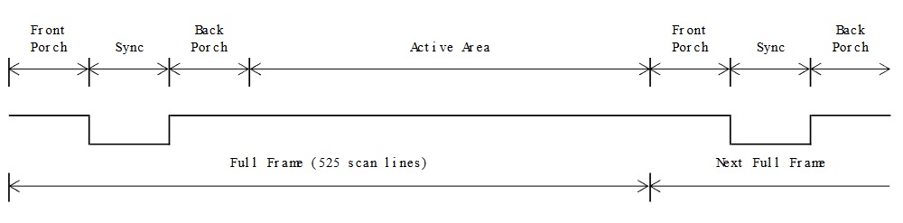
The standard was largely based on the older and well-established NTSC analog television standard, retaining many technical characteristics in order to facilitate the creation of VGA-to-TV converters. It maintained the same vertical resolution of 525 horizontal lines, of which only 480 are visible, while it chose a horizontal scanning frequency of 31.469 kHz, exactly double that of the NTSC standard.
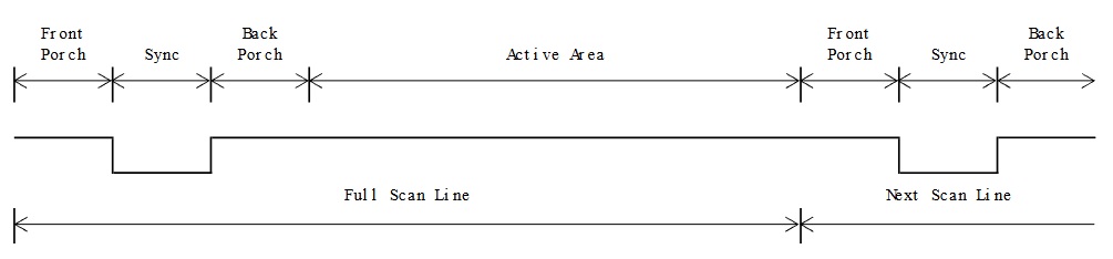
Its operating principle is based on the serial scanning of the screen, line by line (from left to right, from top to bottom). For proper synchronization with the display, two synchronization signals are generated, whose active portion is at a logical low level:
- The horizontal synchronization pulse (HSYNC), which is activated at the beginning of each line
- The vertical synchronization pulse (VSYNC), which is activated at the end of each frame to restart scanning from the top of the screen
In addition, it produces three analog signals with levels ranging from 0 V up to 0.7 V, corresponding to the RGB (Red, Green, Blue) color channels.
The digital signals anatomy
The VGA standard imposes strict specifications regarding the frequency and structure of the generated signal, which consists of two main components: the horizontal and vertical synchronization pulses.
Proper timing ensures the stable and reliable display of the image on the screen, synchronizing the rendering of each line (scanline) and each frame. All the individual time intervals are based on a unified clock frequency, known as the Pixel Clock. The Pixel Clock frequency is 25.175 MHz. Based on this frequency, both the horizontal and vertical refresh rates are calculated, which are critical for the correct refresh of the image on the screen.
The Horizontal SYNC
| Scanline Part | Cycles | Duration (μs) |
|---|---|---|
| Active Area | 640 | 25.42 |
| Front Porch | 16 | 0.64 |
| Sync Part | 96 | 3.81 |
| Back Porch | 48 | 1.91 |
| Scanline | 800 | 31.78 |
The Vertical SYNC
| Frame Part | Lines Count | Duration (ms) |
|---|---|---|
| Active Area | 480 | 15.25 |
| Front Porch | 10 | 0.32 |
| Sync Part | 2 | 0.06 |
| Back Porch | 33 | 1.05 |
| Full Frame | 525 | 16.68 |
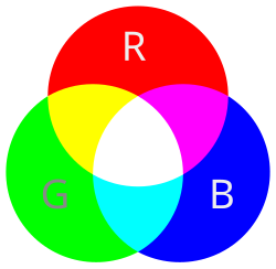
Analog RGB signals
The transmission of color information is carried out through an analog RGB signal (Red, Green, Blue). The overall signal is separated into three independent channels, each carrying the information for one primary color:
- Red channel
- Green channel
- Blue channel
The signal level of each channel ranges from 0.00 V to 0.70 V, where:
| Level (Volt) | Brightness |
|---|---|
| 0.00 | Absence of Color (Black) |
| 0.35 | Medium Brightness Color |
| 0.70 | Maximum Brightness Color |
This range is generated by a digital-to-analog converter (DAC), which converts the digital value of each color into the corresponding analog voltage level. It is evident that three DACs are required, one for each color channel.
The combined activation of the RGB channels leads to additive color synthesis, which enables the creation of a wide overall color spectrum.
Hardware Architecture of the Serial VGA Controller
The VGA controller is implemented using a PIC 18F47K42 microcontroller, squeezing out every bit of its available horsepower through efficient utilization of its peripherals.
The choice of an 8-bit microcontroller was not accidental. While employing a 32-bit ARM Cortex-M device or an FPGA would have made the implementation considerably easier, it would undermine the very objective of the project. The aim was not to build a high-performance VGA controller, but to prove that even a resource-limited microcontroller, when paired with smart peripheral management and disciplined programming, can satisfy the strict requirements of the VGA standard and produce a continuous, flicker-free video signal.
To better illustrate the overall system design, the hardware architectural overview is presented in the diagram below:
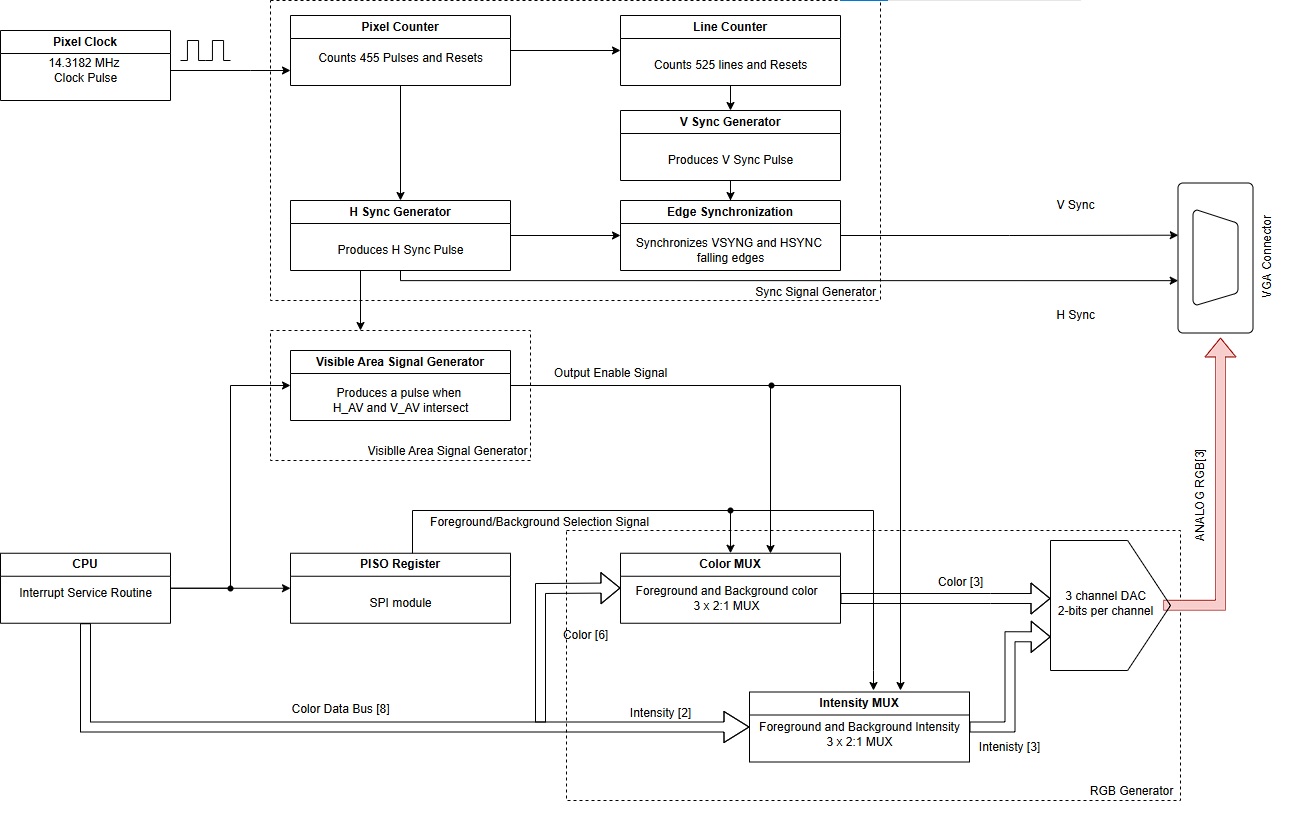
Hardware Architectural Overview
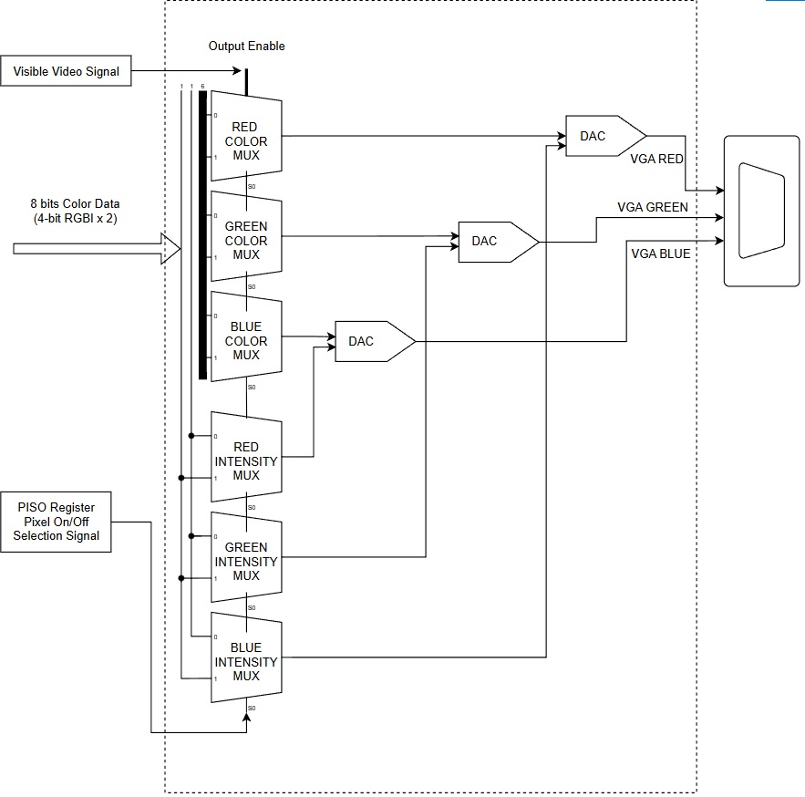
As shown above, the system consists of three major independent functional units, which cooperate to generate all the signals required for driving the display. Specifically, the hardware includes two internal and one external entity. Those are:
-
Synchronization Signal Generation Unit (internal)
Responsible for producing the horizontal and vertical synchronization signals. -
Visible Area Signal Generation Unit (internal)
Generates the intersection of the horizontal and vertical active areas and enables the multiplexers. -
RGB Analog Signal Generation Unit (external)
Implemented outside the microcontroller and includes the multiplexers and digital-to-analog converters that produce the analog RGB signal.
SYNC Signals Generation Unit
The SYNC signals are generated exclusively in hardware using the MCU peripherals. As a result, the microcontroller, operating at 14.3182 MIPS, is able to maintain precise timing for horizontal and vertical synchronization without imposing additional software overhead. This hardware-based generation ensures deterministic signal edges, minimizes jitter, and allows the CPU core to remain available for higher-level tasks.
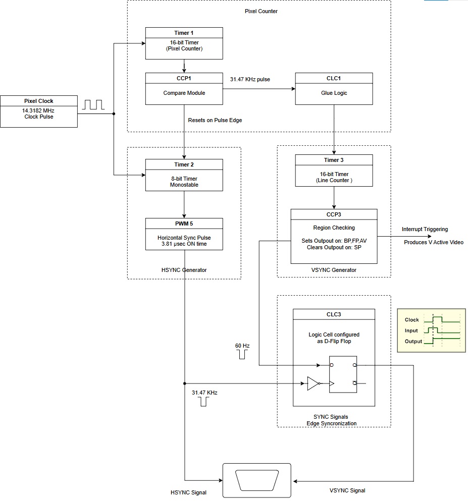
SYNC signals generator
Note that the clock used is not the standard 25.175 MHz. This frequency would be out of specification for the PIC18F47K42, whose maximum supported external clock input is 16 MHz. Instead, given the partial backward compatibility with the NTSC standard, a passive crystal of 14.3182 MHz has been selected. This frequency is commonly used in televisions that support NTSC analog signals and is both widely available and extremely low cost.
The MCU is set to use 4 × PLL internally. However, due to the PIC18 architecture, the system clock is always divided by 4 to obtain the instruction clock OSC / 4.
With a 14.3182 MHz external crystal and the PLL set to 4×, the internal oscillator is 14.3182 MHz × 4 = 57.2728 MHz and the instruction clock becomes (57.2728 MHz) / 4 = 14.3182 MHz.
Therefore, the instruction clock ends up exactly equal to the crystal frequency, and the pixel clock becomes effectively 14.3182 MHz, matching the instruction rate.
By making this choice, the maximum pixel clock frequency corresponds to (14.3182 MHz) / (25.175 MHz) = 56.87% of the standard. Therefore, the cycles corresponding to each scanline will be 800 × 0.5687 = 455.
This ensures perfect alignment with the timing requirements of the standard, since:
455 / (14.3182 MHz) = 31.78 µs, exactly as required by the specification.
At the same time, this choice limits the maximum horizontal resolution, which can no longer exceed 640 × 0.5687 = 364 pixels. Although this value appears significantly lower than the 640 pixels originally supported by the standard, it is nonetheless entirely acceptable for data visualization and, in fact, far exceeds the typical resolutions achieved by 8-bit era computers.
The following table shows the recalculated VGA horizontal timing parameters when the pixel clock is derived from a 14.3182 MHz crystal. Each section has been proportionally adjusted to match the lower clock frequency, while the overall length remains 31.78 µs, perfectly matching the VGA standard’s requirements:
| Section | Cycles | Time (µs) |
|---|---|---|
| Active Area | 364 | 25.42 |
| Front porch | 9 | 0.63 |
| Sync part | 55 | 3.84 |
| Back Porch | 27 | 1.89 |
| Whole line | 455 | 31.78 |
Adjusted HSYNC signal
Visible Area Signal Generation Unit
The Visible Area Video signal is also hardware-assisted, thereby further reducing the processing load on the MCU. It utilizes two PWM modules to generate the required timing intervals:
- The PWM6 unit produces a signal with an active state duration (on-time) of 1.89 µs, corresponding to the Horizontal Back Porch interval.
- The PWM7 unit produces a signal with an active state duration (on-time) of 27.31 µs, equal to the sum of the Horizontal Active Video and Horizontal Back Porch intervals.
The intersection of the inverted PWM6 signal and the PWM7 signal defines the Horizontal Active Video interval. The intersection of this interval with the corresponding interval of the vertical synchronization pulse defines the Visible Video area.
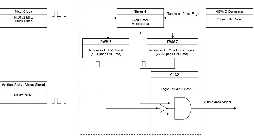
Visible Area Signal Generator
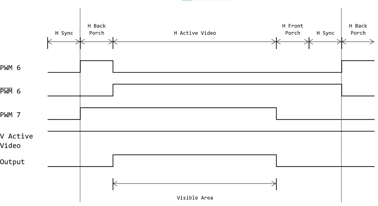
Visible Area Signal - PWM intersection
The VSYNC, the HSYNC and the Visible Area signals, collectively define the complete VGA frame. Pixel data is transmitted to the VGA interface exclusively during the intersection of the H Active Area and V Active Area. An abstract representation is shown below:
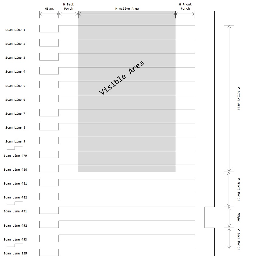
Full VGA Frame
RGB Analog Signal Generation Unit
The VGA controller relies on minimal external hardware, consisting only of two 2:1 multiplexers and a simple R-2R resistor ladder network. These components, together with the microcontroller’s peripherals, form the complete signal path required to generate the VGA output without the need for additional complex circuitry.
For each RGB color channel, two multiplexers are used: one for selecting foreground or background color, and one for selecting low or high brightness intensity. It should be noted that all brightness multiplexers are interconnected, so that the choice of low or high intensity applies simultaneously to all three color channels, effectively changing the signal level produced by the DACs.
In theory, a single brightness multiplexer would be sufficient to drive all color channels. However, after market research, it was found that the 2:1 multiplexers of the 74HC257 and 74AHC257 (high speed) series, which are the most widely available, allow a current flow of 12-35 mA per pin (depending on manufacturer and operating voltage). In addition, the voltage drop at the outputs varies according to the output current. To ensure maximum stability of the output voltage driving the DACs, as well as flexibility in choosing multiplexers from any manufacturer, it was decided to use one multiplexer per color channel. In this way, unwanted variations in signal level are avoided and a more stable color rendering is achieved.
RGB color generator block diagram
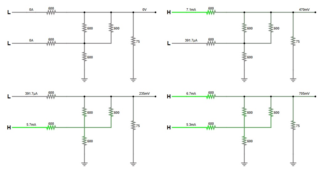
2-Bit R-2R DAC
Note that the 75 Ω resistor in the schematic diagram is the monitor’s input termination and not a part of the on-board 2-bit DAC network.
The outputs of each pair of multiplexers feed the 2-bit DAC of the corresponding color channel. The color information, already quantized into 4 bits, is mapped to 16 discrete levels of analog signal in the range of 0.0-0.7 V, which is then supplied to the display, producing 16 different colors.
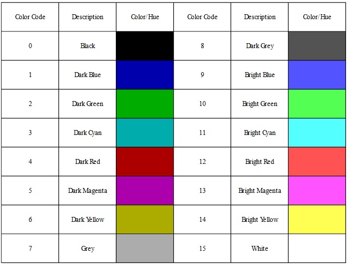
Color Chart
Additonal info can be found in the project's github repository.