Keith
Keith
I looked at a chip that would convert the Y', (R-Y) and (B-Y) signals to RGB, but I think my SCART-input to HMDI upscaler already copes with this. I must confirm,
I so, I may be able to omit much of the copious analogue video circuitry.
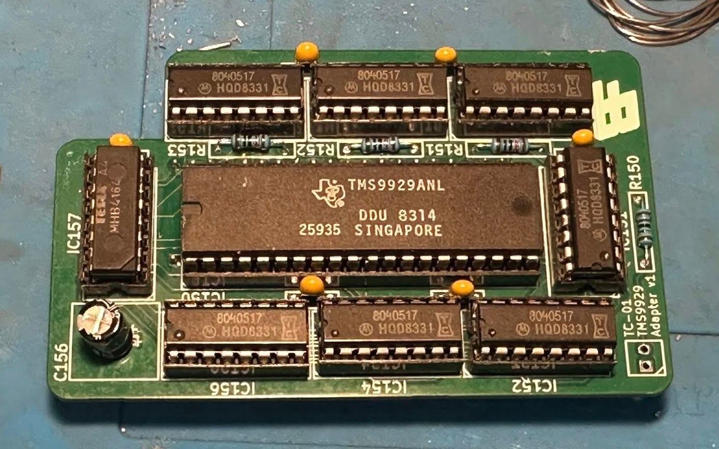
I was gifted a PCB and some parts, so I had to build it into a working toy.
Already have an account? Log in.
To make the experience fit your profile, pick a username and tell us what interests you.

I looked at a chip that would convert the Y', (R-Y) and (B-Y) signals to RGB, but I think my SCART-input to HMDI upscaler already copes with this. I must confirm,
I so, I may be able to omit much of the copious analogue video circuitry.
Assembly
The TC-01 has a lot of board space and analogue circuitry to drive the RF modulator.
I want to bypass as much of this as possible.
The TMS9929 outputs Y, R-Y, and B-Y (component) signals which require a PAL encoder for composite video.
I use a SCART to HDMI upscaler box. These are mass produced for people use their old SDTV gadgets (e.g. DVD players) with modern HDTV screens. This avoids the effort of adding this ability to every retro-computer I have.
My upscaler accepts composite video, RGB and component video. So I thought I would simply need three 75-ohm RF buffers to output component video.
Apparently if you do this, the colours are a bit off, because the colour burst is in the black reference level period of the baseband video signal. See: https://hackaday.io/project/13056-tms9929a-rgb-and-component-adapter
which is a board to solve this issue.
There is a very compact board that produces RGB output and fits underneath the TMS9929. About £37 including postage and VAT.
You can even buy an FPGA replacement, the F18, but at around £65 this is half the cost of a populated board.
I want to keep the total cost less than the cost of buying a populated board.
The TMS9129 is essentially a TMS9929 that uses two 64k x 4-bit DRAM chips instead of eight 64k x 1-bit chips.
This is definitely good for reducing board complexity, and the TC-01 used it, but it has become much scarcer and pricier than the TMS9929. There are several ways to make an adapter board:
This is a bit pointless because 1-bit DRAM chips are still widely and cheaply available.
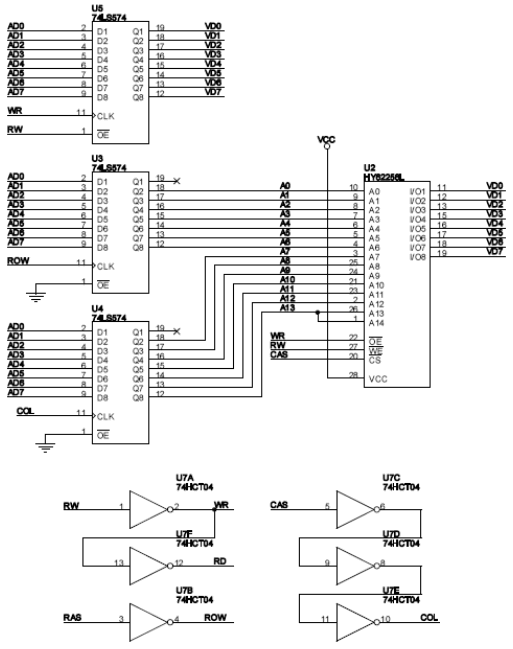
A lot of clever thought by Greg of Digicool things went into this.
This looks the best solution where there are 4-bit DRAM chips already on a host board.
So now I just have to work out how to make the adapter.
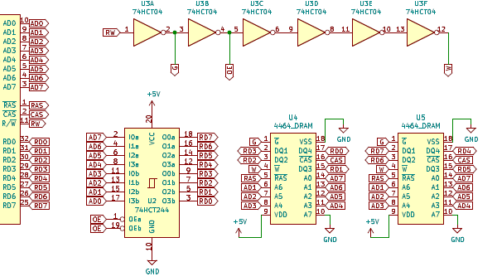
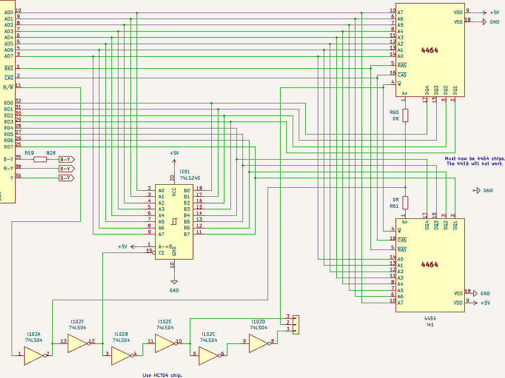
I changed the '244 to a '245, and the inverter gate order to make layout easier.
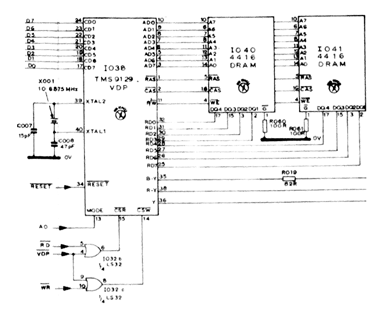
The TC-01 video memory circuit looks like this:
Essentially, we will need to
The 9129 socket has no /G pin, so this signal needs carrying on a flying wire.
The buffer and delay gates could sit on a daughter board, with just one flying wire for /G.
Or they could both sit on the motherboard, with a track cut between R/W and /W.
I had a go at editing Greg's fix into the TC-01 video memory circuit diagram.
R60 and R61 tied /G pins to ground via 100R. They can be omitted,