 Dave
Dave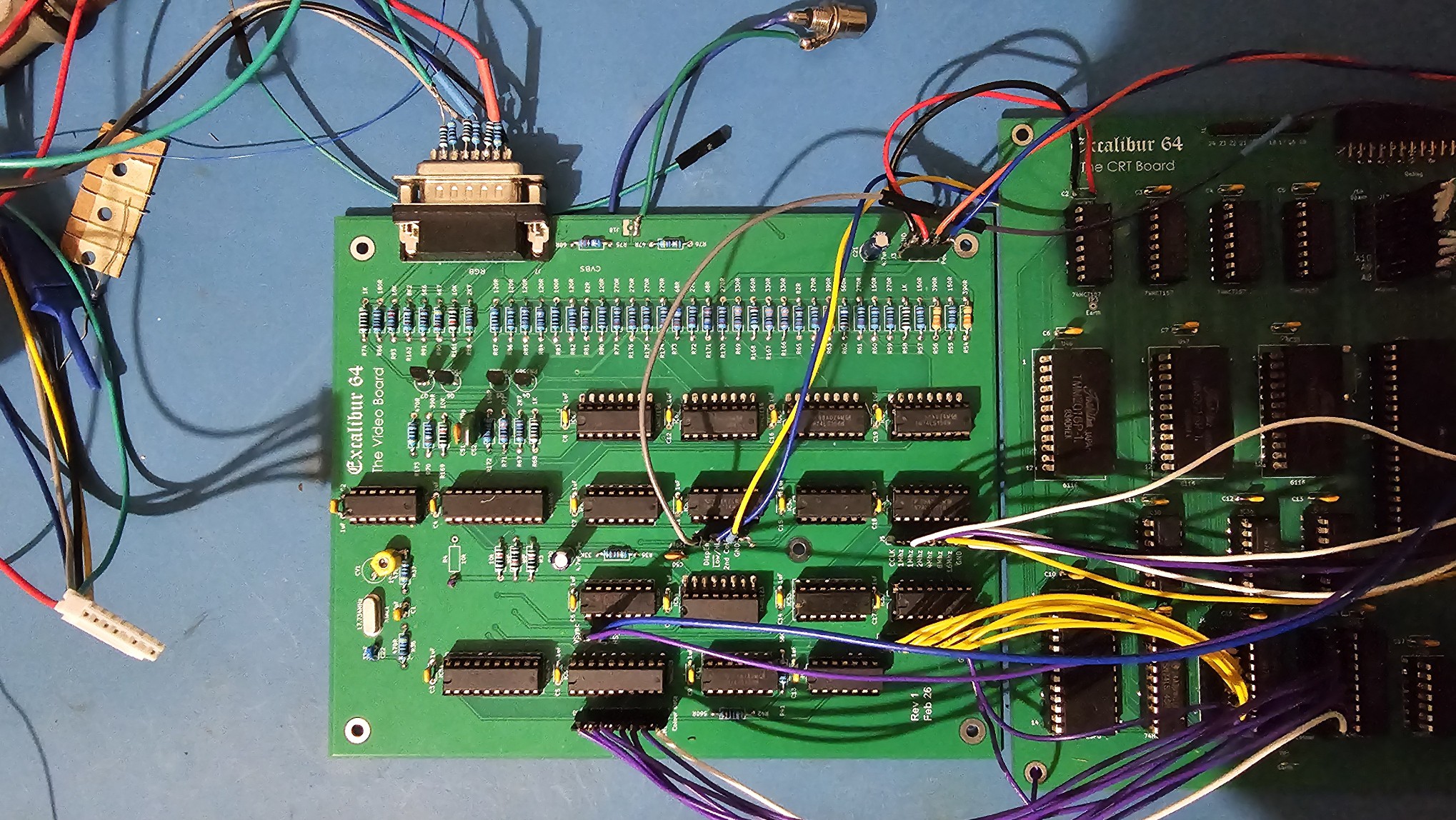
Now that the CRT board (housing the CRTC, SRAM, and character ROM) is finished, it’s time to serialise the dot and colour data. This next stage involves the "Colour, Video & RF Circuit" board. Its job is to convert parallel data into EGA-style signals, composite video, and RF.
While the final build will include an RF modulator, I’m leaving it out for now. I haven't been able to find a new one yet, so I may have to salvage one from a C64. An authentic, static-filled picture will have to wait!
The board features a 15-pin D-sub connector with HSYNC, VSYNC, and two pins for each RGB channel. Although I haven't found official documentation, it’s a safe assumption that this is EGA (specifically 6-bit 'Enhanced' RGB). My plan is to hook this up to a GBS-8200 (EGA-to-VGA converter) first, as getting the composite video working adds a layer of complexity I’d like to avoid for now.
- Clocking: At the bottom of the board, a 74157 divides the main board’s clock frequency and switches between low and high resolution.
- Serialisation: A shift register handles the pixel data serialisation, while an octal buffer drives the 6331 Colour PROM. The 6331 acts as a Colour Look-Up Table (CLUT). Since these are one-time programmable and no longer available, I’ve replaced it with an ATF16V8 (GAL).
- Timing: A 17.734 MHz master clock and 74S04 inverters form a Pierce oscillator for video timing. This provides the high-frequency "dot clock" and is divided down to create the precise PAL colour burst signal. This frequency is exactly four times the PAL subcarrier (4.43361875 MHz).
- Logic: The top row of ICs contains 74156 dual 2-to-4 decoders/demultiplexers with open-collector outputs. These handle the colour mixing, functioning as a DIY Digital-to-Analogue Converter (DAC). They take digital data from the EGA lines (Ra, Rb, Ga, Gb, Ba, Bb) and decode them into specific voltage levels. A resistor ladder is connected to their outputs to create the various voltages representing different colours for the composite and luminance signals.
Installing that ladder was a massive pain—so many different values to keep track of! But finally, the signal passes through an amplifier and buffer stage before exiting via a dodgy-looking RCA connector (I accidentally chose the wrong footprint on the PCB 🫤). So what’s Next?
Next up is testing the EGA output. I didn't actually need to install half of the components for the EGA to work, but the board looked so bare without them! In the next update, we’ll see what happens when I run it through the GBS-8200. I’ll just turn it on and squint my eyes a little—I'm sure it’ll be fine.
Discussions
Become a Hackaday.io Member
Create an account to leave a comment. Already have an account? Log In.