 caspar
## Hardware
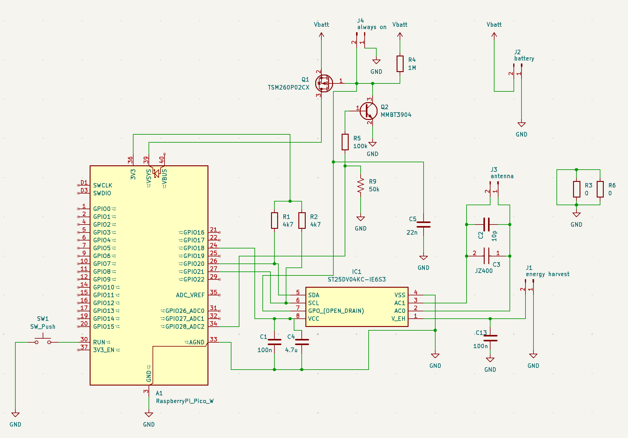
The heart of the circuit is the **ST25DV04KC** — a NFC/RFID chip with an I²C interface. It sits between the phone's RF field and the microcontroller, handling energy harvesting, EEPROM storage, and wake signaling entirely from harvested power.
The ST25 includes a fixed internal capacitor of 27.5 pF (typical) between its antenna inputs AC0 and AC1. A hand-wound loop of 5–6 turns of enameled wire with ~50 mm diameter that provides good coupling to the cell phone yields roughly 3 µH, which with the internal cap alone resonates around 16–19 MHz — above the 13.56 MHz NFC target so that we can tune the antenna into resonance. The external trimmer capacitor C2 is then used to tune the circuit into resonance at 13.56 MHz. The ciruit has all the tools for that onboard: a dedicated tuning firmware samples the harvested voltage V_EH continuously via the Pico ADC and renders a live bar graph over USB serial into the terminal, making antenna optimization straightforward. An ascii tuning tool! Below you see a video capture of me tuning the trimmer cap across resonance, my cell phone with a generic nfc app is at a constant distance to the antenna during tuning.
The **wake/latch circuit** uses a P-MOS high-side switch (TSM260P02CX) to gate battery power to the Pico. The ST25 GPO pin — open-drain, powered from the RF field — pulls the gate low on an EEPROM write event, switching the Pico on. The Pico immediately latches itself via a small NPN (MMBZ390A) to hold power through the command execution, then releases the latch when done.
The PCB breaks out three functional areas: the NFC tag and antenna matching network (center), the power switching and latch circuit (left), and an energy harvest output header (right) for measuring or using V_EH directly.
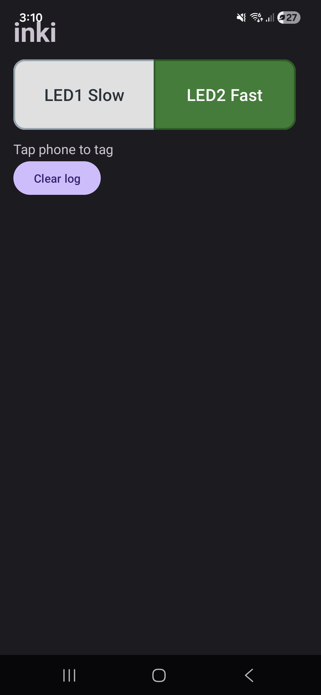
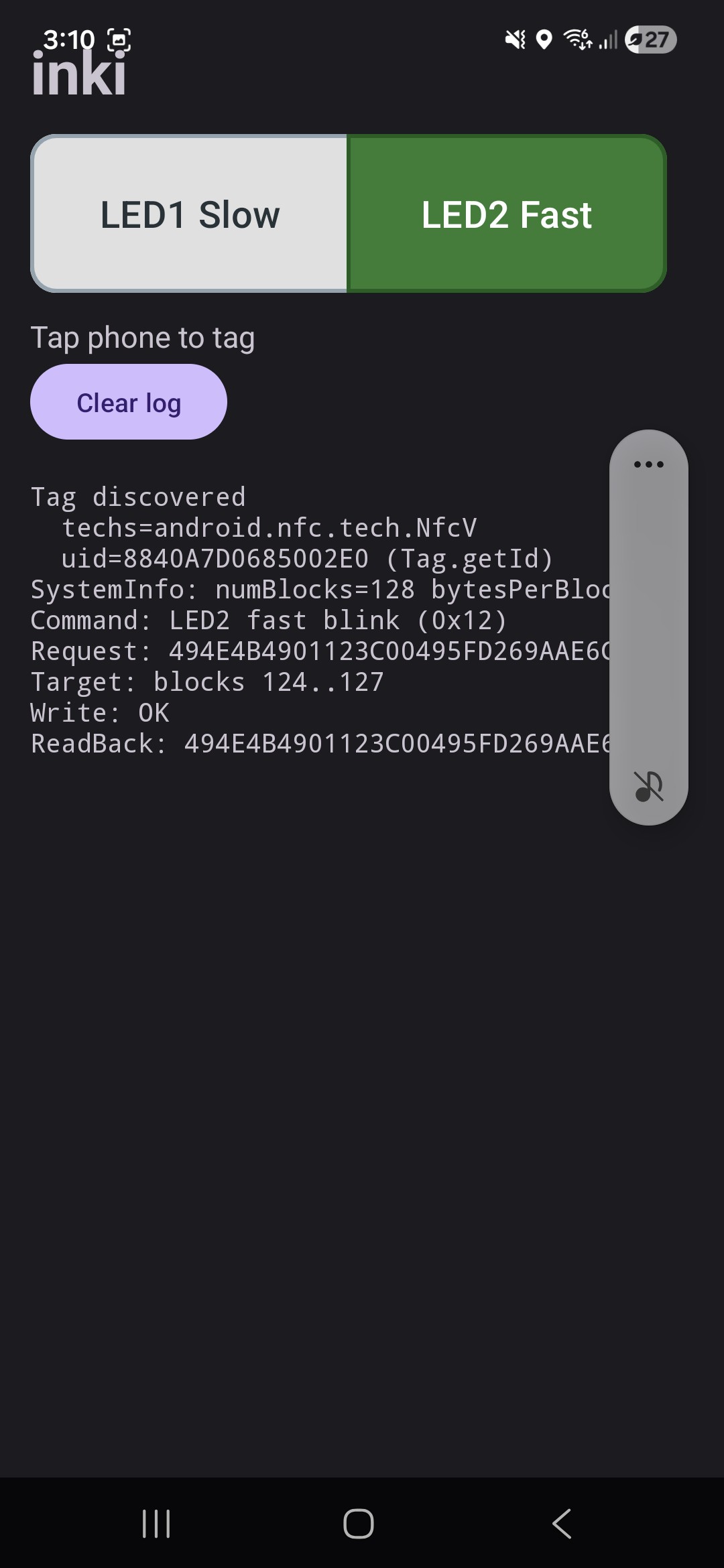
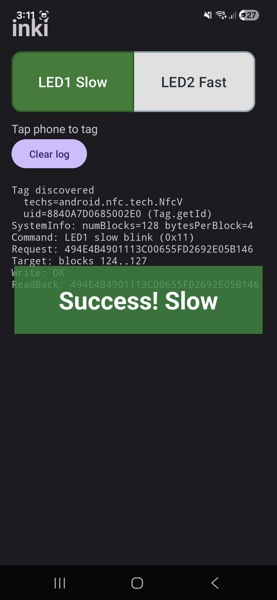
I also used this to wake up my epaper display device inki, as for example to display a custom message:
A simple Android App defines the payload to be transmitted:

 Silícios Lab
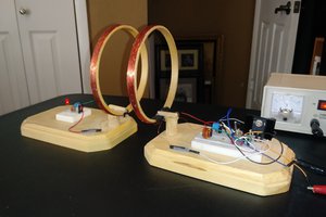
 G. Rosa
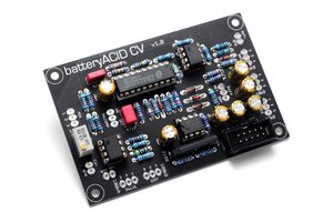
 engineerkid1
 bornach