 Juan Flores
The idea to create this module came a few months ago while I was working with the OV2640 (ESP Camera). Keeping in mind that it can be used with an MCU and that the image quality is decent for some scenarios, it could be considered a good option. However, the main problem I faced was the idle consumption. The sensor has a low-power mode, but for a battery life of one year, it wasn't enough.
So, relays came to mind, which is obviously not a great solution, but that is more or less where the idea originated. Something that allows the device to stay in sleep mode most of the time and wake up periodically, enabling the use of more power-hungry devices for months or even years.
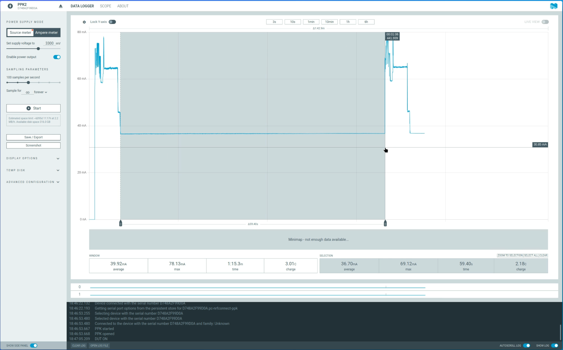
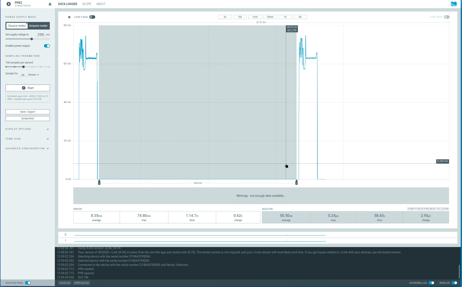
But before continue I'll give you some juicy info to judge by yourself if this is interesting or not:
- Idle consumption with deep sleep mode: 36,7mA
- Idle consumption with this module: 50nA
734.000 times less idle consumption!
Demo note at the bottom.
| Sleep mode | PowerTimer |
 |  |
But less continue with design.
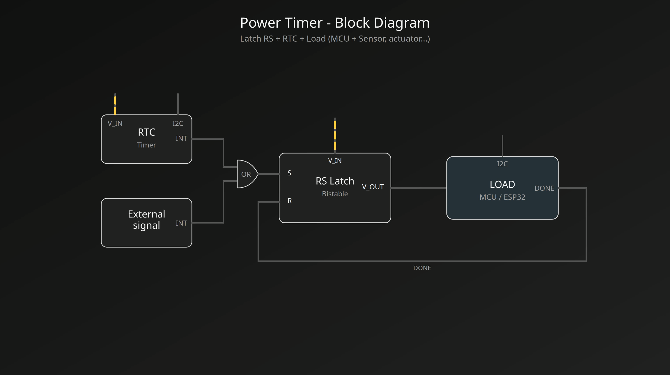
The idea is as follows:
The latch provides energy to the MCU, sensors, and modules. We do some processing; once it's done, we program the RTC and raise the DONE signal. When the RTC alarm triggers, it sets a high level to the SET pin and starts the cycle again. On the other hand, if we have an external module, we could have asynchronous wakeups based on specific conditions.
The architecture is the following:
- Latch R/S: This block manages the energy, allowing it to be provided or cut. Since it's a quite classic circuit, I've decided to implement it manually using passive components and transistors. This implementation is cheaper and allows for fine-tuning the consumption.
- RTC: This component is key because it's on all the time, so I needed to find something very efficient. I've chosen the RV3028-C7. This RTC has a consumption of 45 nA, allows three separate types of events: timers, alarms, and external interruptions (not implemented in this part).
- OR gate with diodes: I don't know if it's some kind of consumption paranoia, but I've implemented a simple OR gate with diodes to connect the RTC interrupt output, a button, and a possible external interruption.
LATCH R/S:
This is a standard R/S LATCH but with a couple of modifications, though nothing serious. First, here is a definition:
An R/S latch is a fundamental building block in digital electronics that uses feedback to hold a stable state. When the S (set) input is activated, the output Q becomes 1. When the R (reset) input is activated, Q becomes 0. When both inputs are inactive, the latch keeps its previous state. Certain input combinations (depending on implementation) may be considered invalid.
So, in summary, it is like a switch with two buttons: one allows the energy flow and the other cuts it.
Regarding the modifications or relevant parts, I would highlight the first one:
I've used an AO3401A P-Channel MOSFET. It might be a bit oversized, with up to 30V VDS and a max current of 4A, but it is quite cheap. I've split the tracks on the DRAIN and SOURCE to improve heat management. Regardless, I've tested it with a load of 1A, and it looks safe to use.
The final modification is at the SET input; I've added another MOSFET to work as a switch. This way, if we have a high level at the RESET signal, it won't allow both to be active at the same time, preventing an uncertain state caused by both signals being high.
RTC:
This component's primary purpose is to produce periodic or programmed interruptions to wake up the system by raising a signal on the SET pin.
I've chosen the RV-3028-C7. The most relevant features are the following:
Ultra-low power consumption in working mode: around 45 nA!
Wide voltage range, from 1.1V to 5V. This range defines the module's voltage range, but I think it's a useful range for most scenarios.
Timer, Alarm, and external interruptions. These options are independent, so you can use all of them at the same time. The only thing to keep in mind...
Read more »