 Marco Tabini
The signaling that takes place on the CC lines of a USB-PD connection is very interesting. For starters, despite the fact that there are two CC lines, only one of them is used for USB Power Delivery communication at any given time. The other line may be used as VCONN to power electronically marked cables and certain types of accessories.
Therefore, a traditional clock-and-data signaling scheme is not possible. Instead, the USB-PD specification uses a modulation scheme called biphase mark coding (BMC for short), which is a type of self-clocking code. In this scheme, every bit period contains a transition that helps maintain synchronization between the transmitter and receiver. A logical '1' is represented by an additional transition in the middle of the bit period, while a logical '0' is not. Because transitions themselves carry information, the receiver can recover both the data and the timing from a single wire.
If you've never dealt with self-clocking protocols before, it can be a bit tricky to wrap your head around BMC at first, particularly because it's not trivial to decode without the help of dedicated hardware. However, once you understand the basics of how it works, it's not too hard to deal with, particularly because it operates at a relatively low data rate (up to 300 kbps, compared to the USB data lines, which can reach into the tens of Gbps).
Proximity and crosstalk
However, it's important to understand the environment in which the CC lines operate. In a practical implementation, power-delivery communication and USB data are happening both simultaneously and independently. This means that the controller shaping the USB data signal is not aware of when transmissions are taking place on the CC lines, and therefore cannot coordinate with them in any way.
When you consider that the wires carrying the USB data and CC signals are in close proximity inside a cable, some degree of crosstalk between them is inevitable. While the BMC signaling rate itself is relatively low, excessively sharp transitions can generate high-frequency energy that couples into the adjacent data pairs, reducing signal integrity and noise margins. This is particularly important for USB 3.x and USB4, which operate at very high data rates and therefore require excellent signal quality to maintain reliable communication.
It's the edges that matter
At first glance, you might think that a 300 kbps signaling scheme would be too slow to cause any meaningful interference. However, the frequency content of a signal is determined not only by its data rate, but also by the speed of its transitions. A square wave with very sharp edges contains significant energy at frequencies far above its fundamental frequency, extending well into the hundreds of megahertz and beyond.
As a result, even though USB-PD signaling operates at only a few hundred kilobits per second, poorly controlled edges can still generate enough high-frequency energy to interfere with nearby high-speed signals.
To mitigate this problem, the USB-PD specification requires a technique known as edge shaping. Rather than transitioning between states as quickly as possible, the transmitter intentionally limits the slew rate of the signal so that the rise and fall times occur over a controlled period. You can see this in the oscilloscope capture below, taken during a USB-PD negotiation.
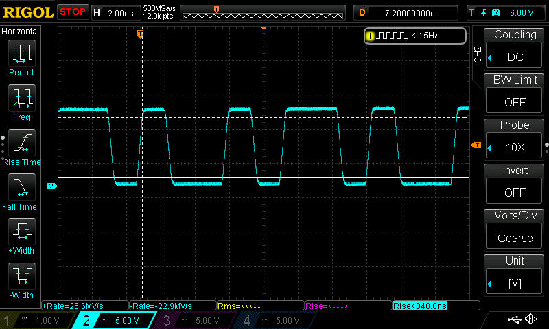
Note how the transitions between high and low states are not perfectly vertical, but instead have a distinct slope. The specification requires a minimum rise and fall time of 300 ns and also imposes upper limits to ensure reliable communication. While 300 ns may seem like a significant amount of time—roughly 10% of a bit period—it dramatically reduces the amount of high-frequency energy generated by the signal. As a bonus, it also reduces electromagnetic interference (EMI), which helps devices meet regulatory requirements.
Implementing edge shaping
Commercial USB-PD controllers typically implement edge shaping directly in their PHY circuitry using dedicated mixed-signal hardware. This allows them to meet the specification's timing requirements without requiring the microcontroller to precisely control the waveform in software.
If you're implementing a USB-PD controller using discrete electronics, however, reproducing this behaviour can be more challenging. Generating a spec-compliant, edge-shaped waveform entirely in software would require extremely precise timing, and any software-induced jitter could affect interoperability with commercial devices.
Fortunately, the same functionality can be achieved relatively easily using a small amount of analog circuitry.
What's edge shaping anyway?
The basic idea behind edge shaping is that, instead of transitioning from one state to another as quickly as possible, you intentionally control the rate at which the voltage changes. The goal is to produce a waveform that more closely resembles a trapezoid than an ideal square wave, reducing the high-frequency components that would otherwise be generated by extremely fast transitions.
From a circuit perspective, this means controlling the current that charges and discharges the capacitances present on the CC line. Since the rate of change of voltage across a capacitor is directly proportional to the current flowing into it, limiting that current allows the slew rate of the signal to be controlled.
A simple resistor-capacitor (RC) network can often be sufficient to satisfy the specification, but it provides only limited control over the resulting waveform. Because capacitors charge and discharge exponentially, the transition rate varies throughout the edge, making it difficult to achieve a predictable waveform shape.
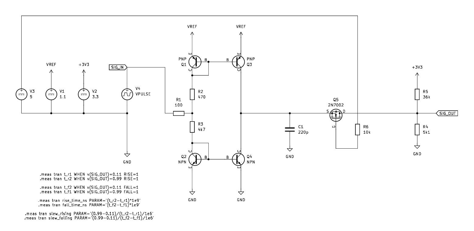
For this design, I wanted more precise control over the slew rate. A much more predictable approach is to use a set of current mirrors to regulate the current flowing during the transitions. This allows the rise and fall times to be controlled more accurately and produces a very clean waveform with only a handful of transistors and resistors:
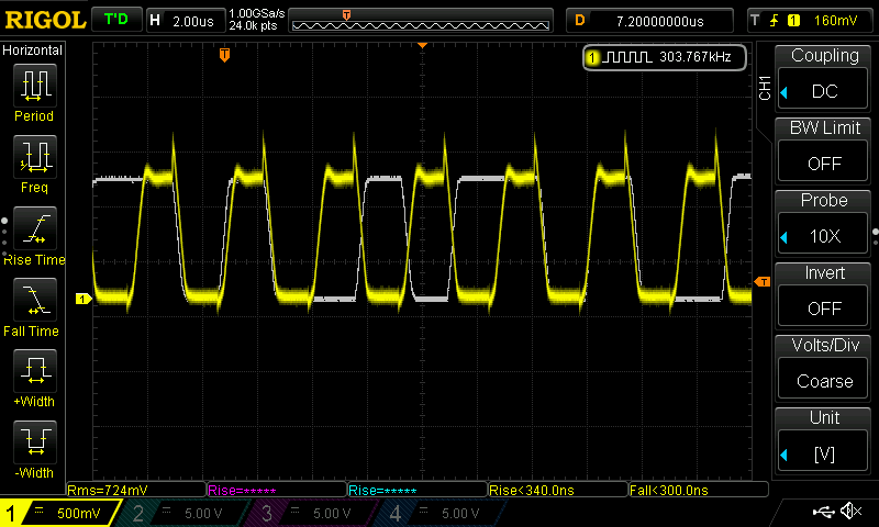
And the resulting signal now looks a lot cleaner, with the desired trapezoidal shape (and a few artifacts due primarily to the fact that I built the circuit on a protoboard and use terrible probing technique):
Discussions
Become a Hackaday.io Member
Create an account to leave a comment. Already have an account? Log In.