 Arnov Sharma
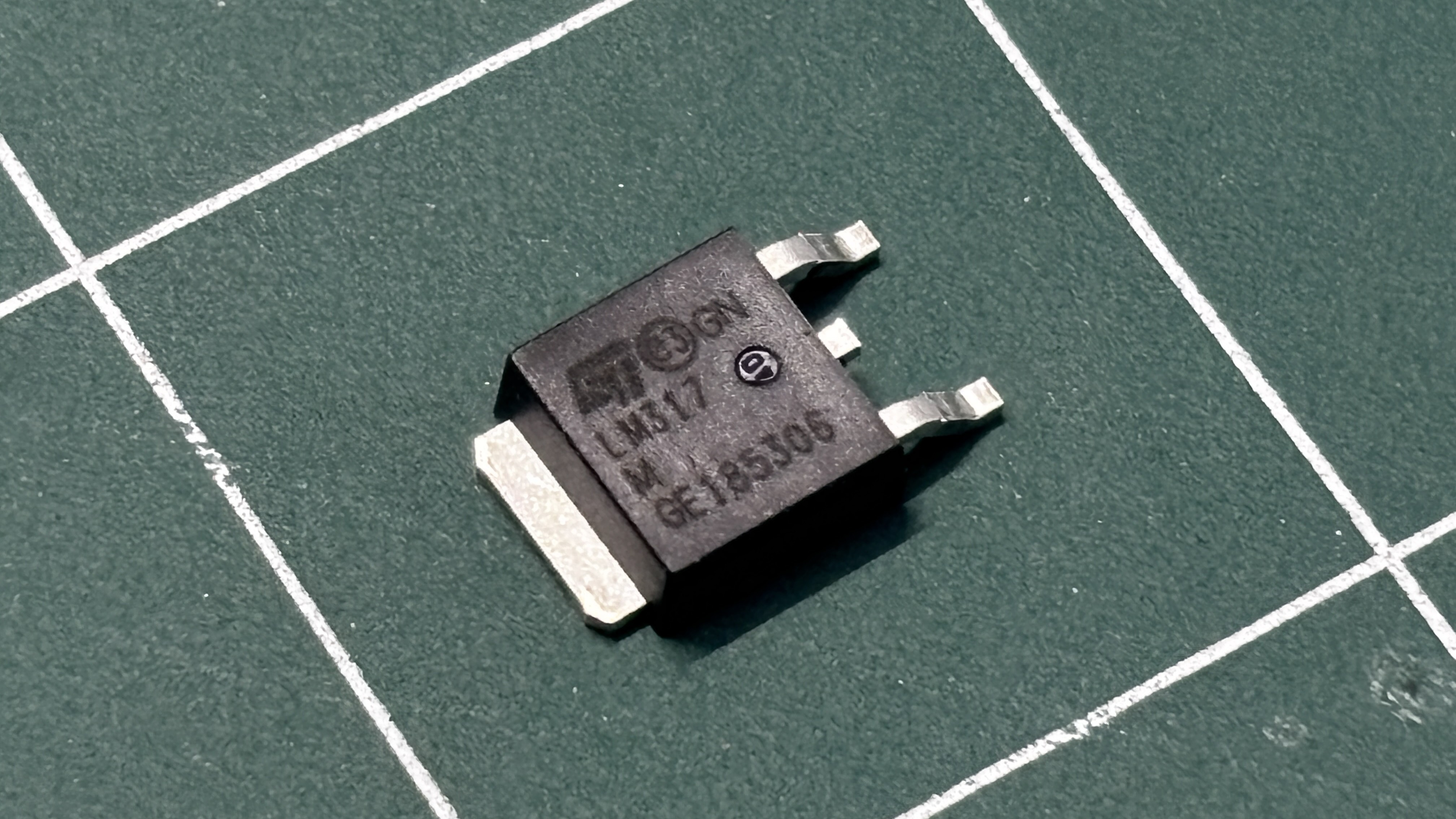
The LM317 is an adjustable linear regulator widely used to derive stable output voltages from a higher DC source. It operates by maintaining a constant 1.25V reference between its output and adjust pins, allowing the output voltage to be precisely set using a pair of external resistors.
It is a three-pin, positive-voltage regulator capable of supplying more than 1.5A over an output voltage range of 1.25V to 37V.
The device requires only two external resistors to set the output voltage and offers excellent performance, with typical line regulation of 0.01% and load regulation of 0.1%.
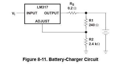
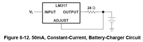
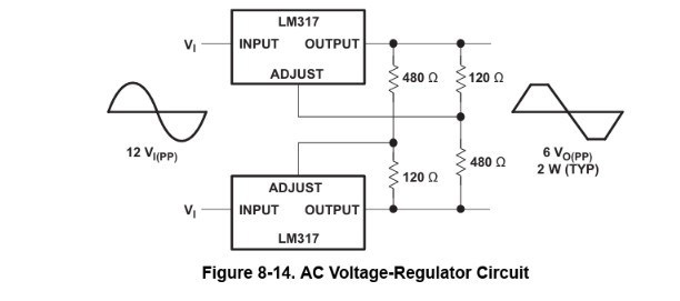
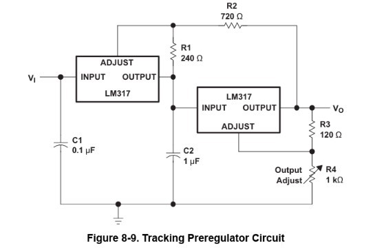
The LM317 is a highly versatile linear regulator that can be used in numerous applications. It can be configured as a standard voltage regulator, a constant current source for battery charging, a tracking pre-regulator circuit, or even an AC voltage regulator circuit.
It also includes built-in current limiting, thermal overload protection, and safe operating area protection, ensuring reliability even under fault conditions. Overload protection remains functional even if the adjust pin is disconnected. Typically, no capacitors are required unless the device is placed far from the input filter capacitors, in which case an input bypass capacitor is recommended. An optional output capacitor can be added to improve transient response, and bypassing the adjust pin further enhances ripple rejection.
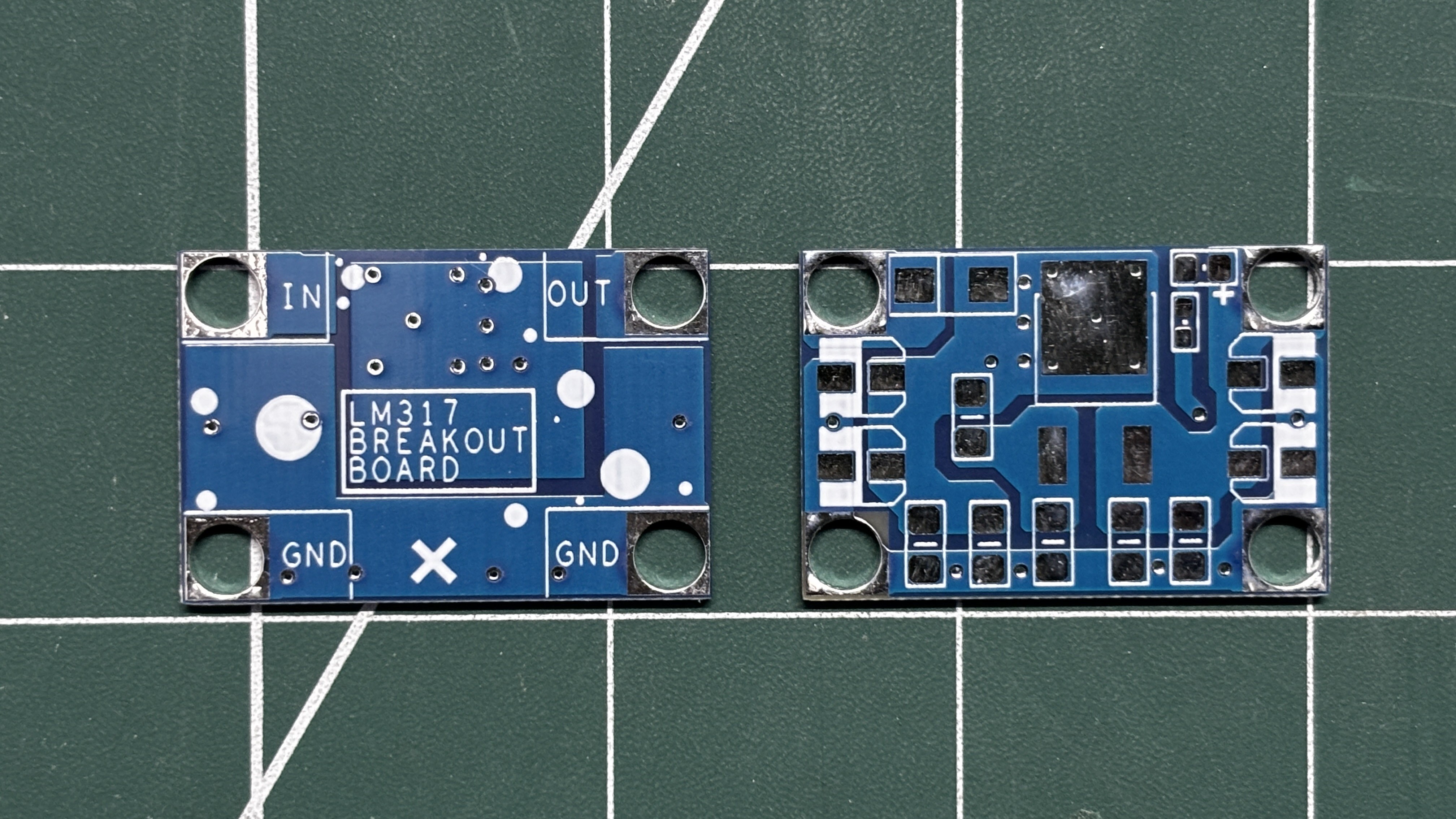
For our circuit, we are using the DPAK (TO-252) footprint, which keeps the design compact while still handling decent power. One of the key advantages of this package is the large exposed tab (internally connected to the output), which can be soldered directly onto a wide copper area on the PCB. This effectively turns the PCB itself into a heatsink, helping dissipate the heat generated due to the voltage drop from 12V to 5V. This approach allows for a clean, space-efficient design without needing bulky external heat sinks while still maintaining good thermal performance.
Check out the Datasheet for more info.
https://www.ti.com/lit/ds/symlink/lm317.pdf
PCB DESIGN
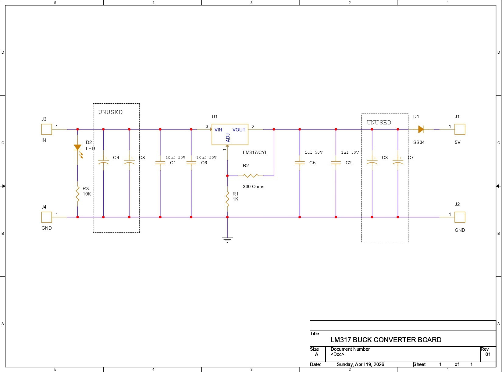
We began the project by preparing the schematic for the buck converter board. We did this by studying the LM317 datasheet and creating a simple schematic that included the LM317 setup with two adjustable resistors connected between the adjust pin and the output pin of the LM317. To ensure stability and reduce noise, we added a 10µF SMD capacitor at the input and a 1µF capacitor at the output, which helps smooth fluctuations and improve transient response. We also added extra capacitor footprints at both the input and output in case different-value capacitors are needed later. The output voltage is configured using a resistor divider (330Ω and 1kΩ), which sets the desired voltage reliably.
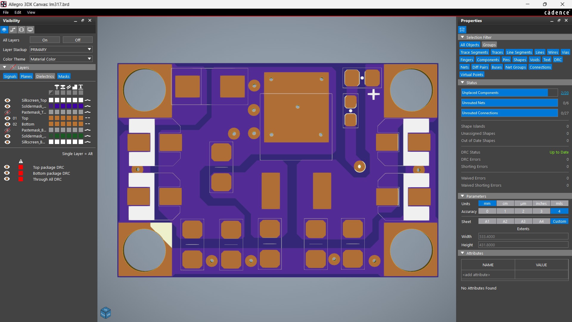
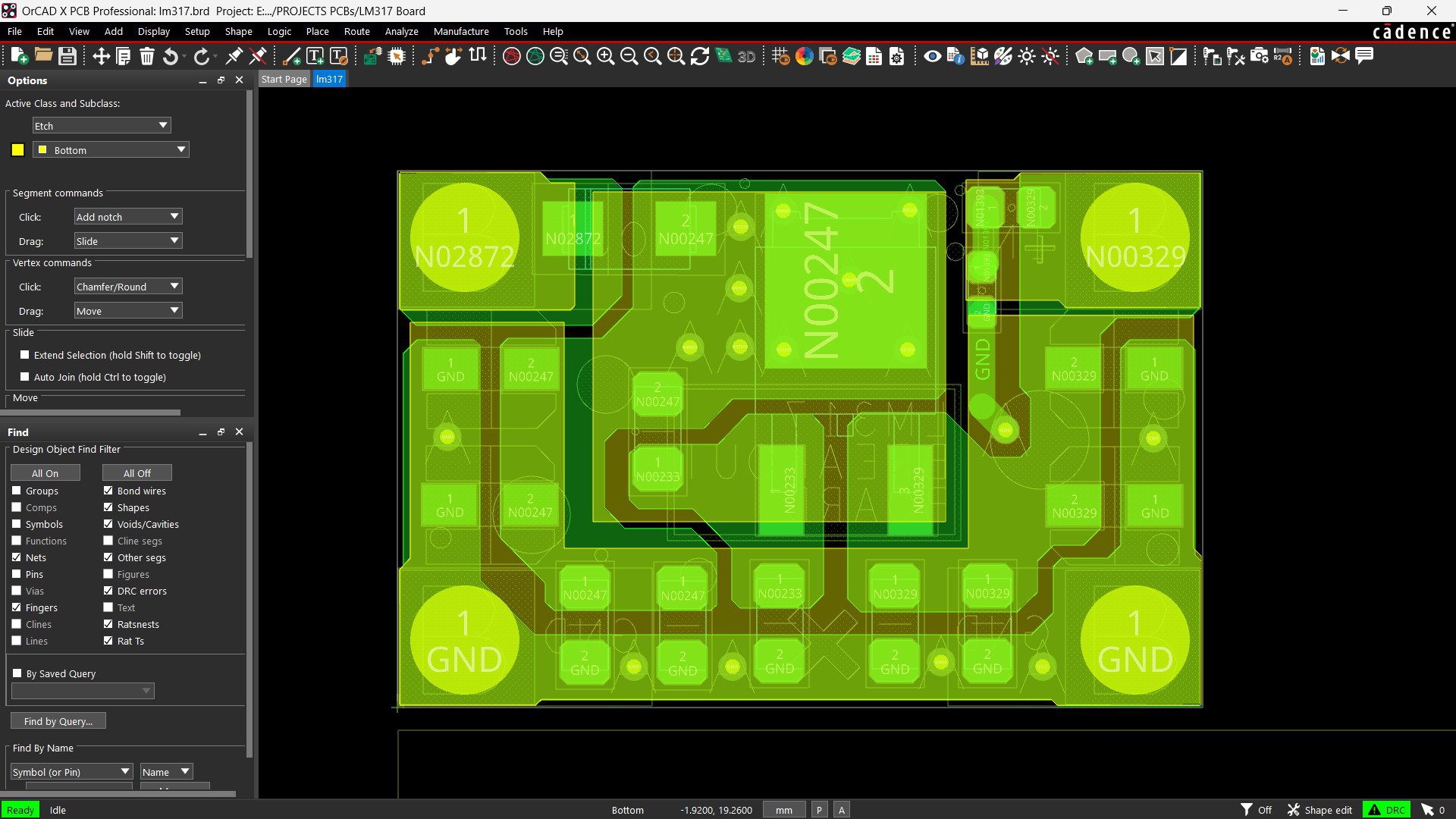
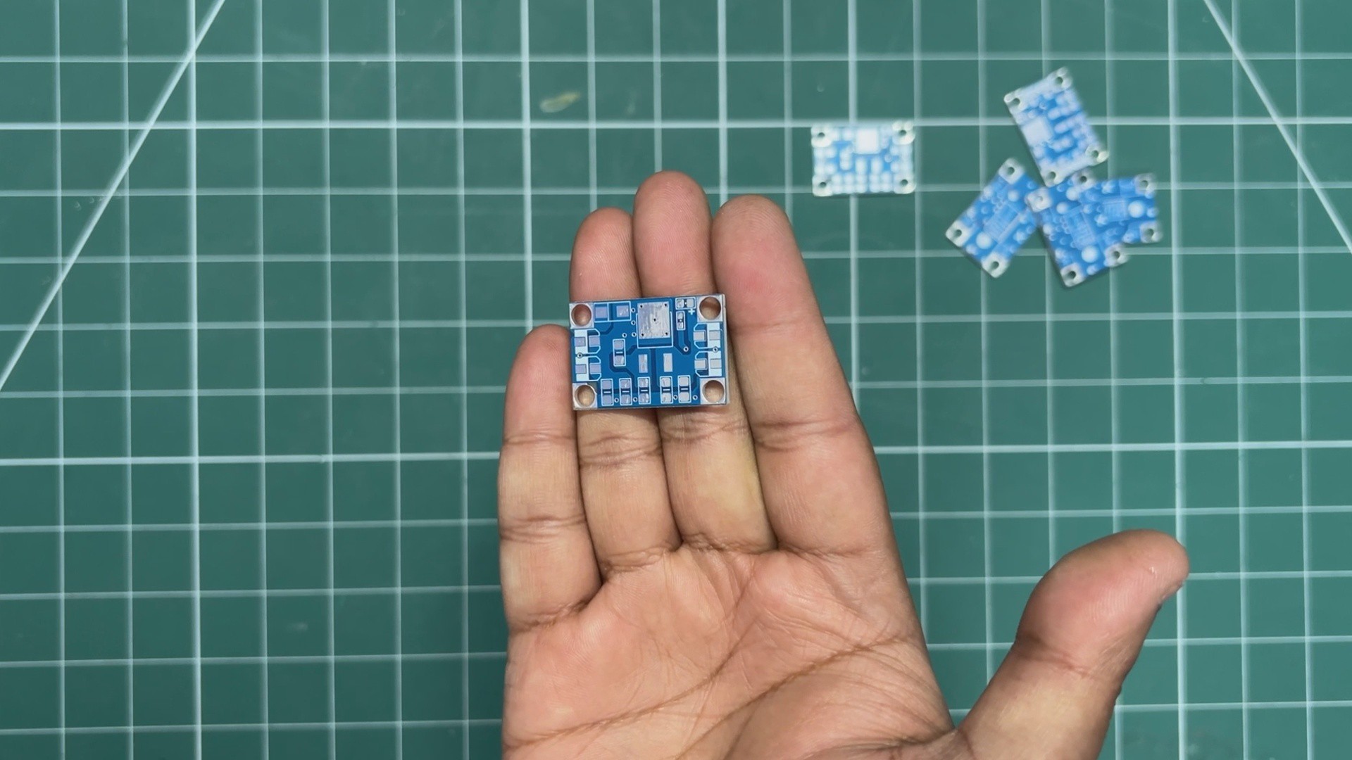
After finalizing the PCB schematic, we exported the data and converted it into a PCB layout. The PCB editing process began by adding all the components to the PCB design first. We used all SMD components for this project, including 1206 package capacitors, 1206 package resistors, and a DPAK (TO-252) LM317. We prepared a small board of size 20mm x 30mm and placed all the components within this board. We added four CON1 terminals for the VIN, VOUT, and GND pins, placing them along the edges of the board outline. Two CON1 pads were placed on the right side for the input, and two CON1 pads were placed on the left side for the output.
After finishing the placement, we connected all the net lines and completed the board layout.
After finalizing the PCB design, we exported the Gerber files along with the NC drill files and shared them with NextPCB to get the samples manufactured.
NextPCB PCB SERVICE
After completing the PCB design, Gerber data for the PCB was sent to HQ NextPCB, and an order was placed for Blue Solder mask boards with a white silkscreen.
After placing the order, the PCBs were received within a week, and the PCB quality was pretty great.
In addition, I have to bring in HQDFM to you, which helped me a lot through many projects. Huaqiu’s in-house engineers developed the free Design for Manufacturing software, HQDFM, revolutionizing how PCB designers visualize and verify their designs.
Take advantage of NextPCB's Accelerator campaign and get 2 free assembled RP2040-based PCBs for your innovative projects.
https://www.nextpcb.com/blog/rp2040-free-pcba-prototypes-nextpcb-accelerator
This offer covers all costs, including logistics, making it easier and more affordable to bring your ideas to life. SMT services can be expensive, but NextPCB is here to help you overcome that hurdle. Simply share your relevant project, and they'll take care of the rest. Don't miss out on this amazing opportunity to advance your tech creations!
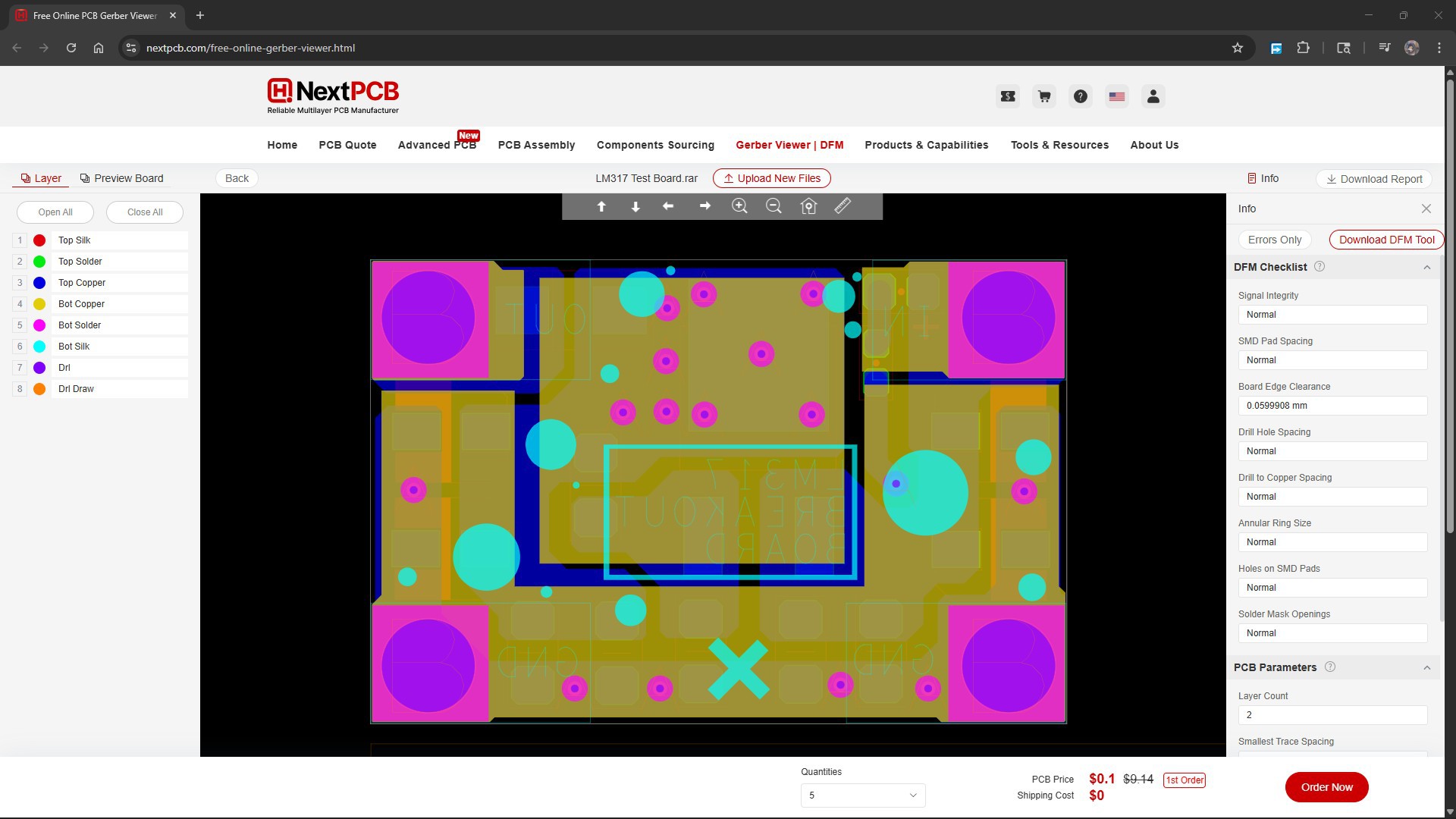
HQDFM: Free Online Gerber Viewer and DFM Analysis Tool
Also, NextPCB has its own Gerber Viewer and DFM analysis software.
Your designs are improved by their HQDFM software (DFM) services. Since I find it annoying to have to wait around for DFM reports from manufacturers, HQDFM is the most efficient method for performing a pre-event self-check.
This is what I see in the online Gerber Viewer. It's decent for a quick look, but not entirely clear. For full functionality—like detailed DFM analysis for PCBA—you’ll need to download the desktop software. The web version only offers a basic DFM report.
With comprehensive Design for Manufacture (DFM) analysis features, HQDFM is a free, sophisticated online PCB Gerber file viewer.
With over 15 years of industry experience, it offers valuable insights into advanced manufacturing processes. If you’re looking for reliable PCB services at a budget-friendly price, HQ NextPCB is definitely worth checking out.