 Allan Binder
With the schematics drawn and parts sorted into their labeled bins, it was finally time to start populating a breadboard. The plan was to build the entire digital chain first; pulse shaping, stretching, re-squaring, and the coincidence AND gate. Without any of the analog front-end and definitely without any HV anywhere on the bench.
I'll spoil the post: it was uneventful. Which is the goal, honestly. The fun part of breadboard work is that satisfying click of components going into rows and the slow accumulation of a circuit that starts to look like the schematic on paper. Two 74HC14s, a 74HC08, a 100nF decoupling cap on every IC's VCC pin (every IC!!), the BAT54 diodes and RC networks for the stretchers, all the bias and pull-down resistors. About an hour of work, a couple of moments where I had to recount pin numbers, and a finished chain.
A few small choices worth calling out:
The BAT54s are SOT-23 SMD parts, which is annoying on a breadboard. I soldered short lead wires onto each one before plugging them in. Ugly but functional, and they'll be replaced with through-hole packages once the design moves to PCB anyway.
I tied all unused 74HC14 and 74HC08 inputs to ground rather than leaving them floating. CMOS inputs that float pick up noise and can self-oscillate, which is exactly the kind of subtle problem you don't want chasing later when the analog side is also misbehaving.
I left the cathode pulse inputs (TUBE1_RAW and TUBE2_RAW on the schematic) terminated at unused breadboard rows for now. Those will get connected to the GM tubes once the analog front-end exists. Until then,they're just landing pads waiting for a signal.
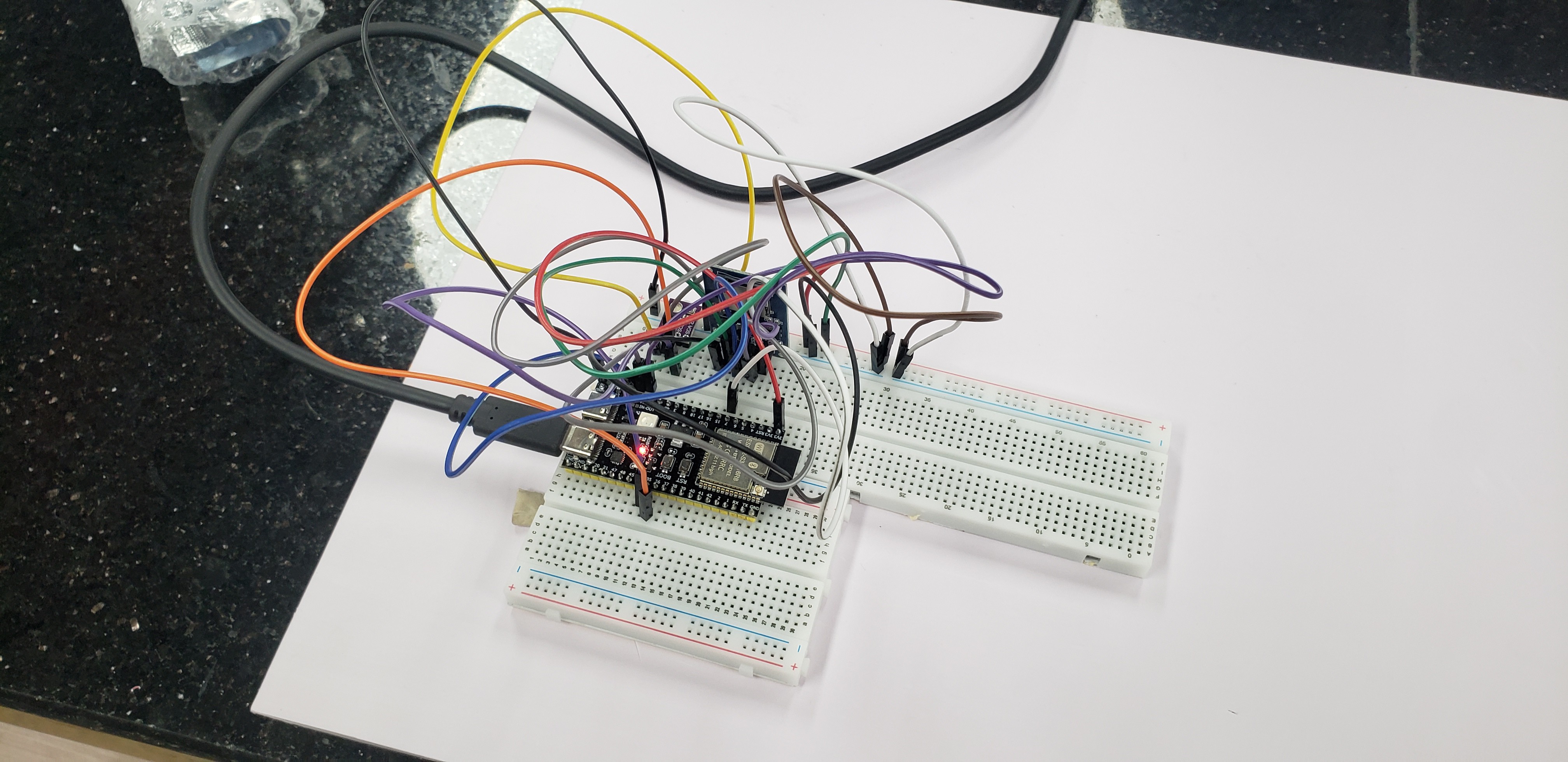
Next post is going to be the more interesting one: validating that the chain actually works using synthetic pulse injection. I'm generating test pulses from an ESP32 GPIO and walking through the chain stage-by-stage with a logic analyzer to make sure each transformation happens the way the schematic says it should. That's the post where I find out if I drew the circuit correctly.
Discussions
Become a Hackaday.io Member
Create an account to leave a comment. Already have an account? Log In.