Close
0%
0%

GadgetSci MCA

A 4096-ch MCA for gamma spectroscopy. i.MX RT1010, external ADC via DMA, SiPM bias supply. Open hardware. Launching on Crowd Supply.

Similar projects worth following
0 followers
GadgetSci MCA is a compact, open-hardware gamma spectroscopy acquisition board. Real-time pulse detection, peak height analysis, energy extraction, and 4096-channel histogramming run entirely on an i.MX RT1010 Cortex-M7 at 500 MHz. External ADC clocked via DMA. Onboard configurable SiPM bias supply. ~100 g, battery-capable.
This page is the lab notebook: scope captures, measured data, schematic details, failures.
Full project story and build logs:
- Hackster.io — coming soon
- Crowd Supply pre-launch: https://www.crowdsupply.com/andak-consulting/gadgetsci-mca

GadgetSci MCA

Compact, open-hardware gamma spectroscopy acquisition board. Real-time peak detection, energy extraction, and 4096-channel histogramming on an NXP i.MX RT1010 Cortex-M7 at 500 MHz. Onboard configurable SiPM bias supply. ~100 g, battery-capable.

Pre-launch page: Crowd Supply

Signal Chain

Gamma ray hits a scintillator crystal, producing a flash of visible light. A SiPM optical sensor detects the light and outputs a current pulse. A front-end amplifier inside the detector converts and amplifies this signal. Inside the MCA, an analog peak detector captures the pulse amplitude and holds it. An ADS7042 (12-bit, 1 MSPS) digitizes the held value. The RT1010 reads the result, sorts it into one of 4096 energy bins, and resets the peak detector capacitor for the next pulse.

Pulse detection is threshold-based: an analog comparator with a voltage reference triggers acquisition. No RTOS — bare metal firmware on the RT1010.
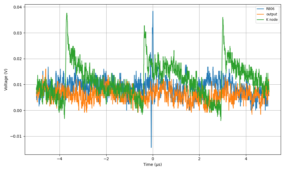
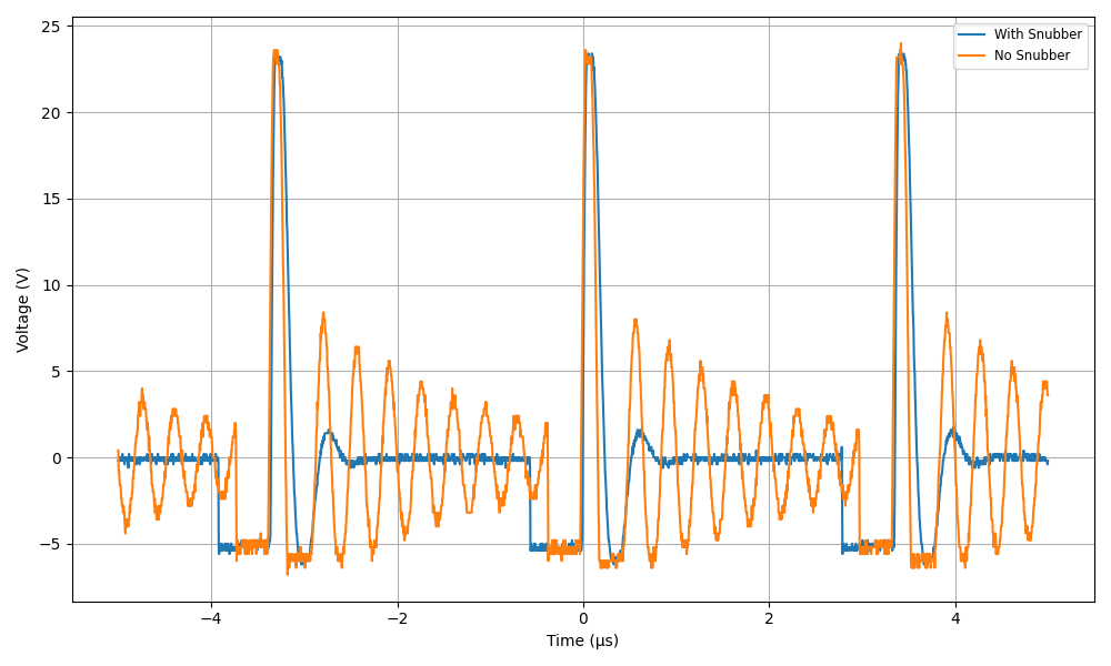
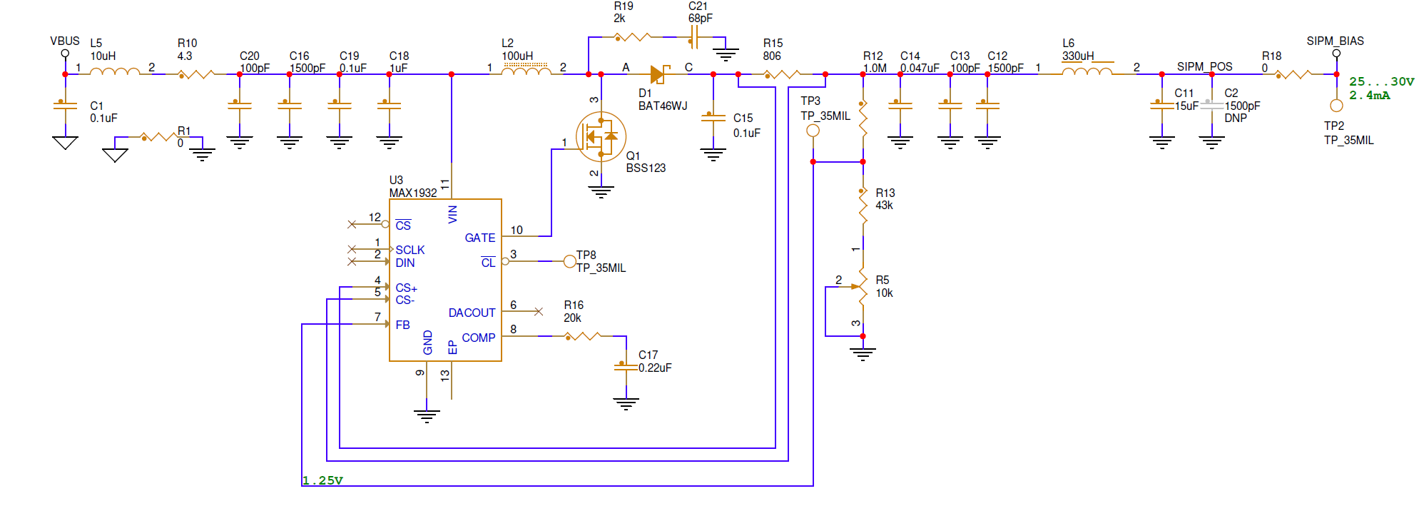
Bias Supply

The MCA provides the SiPM bias voltage onboard — 25–30V, a few mA, DAC-controlled over SPI via a MAX1932 in boost/discontinuous mode. This is what makes the system portable; no external supply needed.

Hardware

Rev B is the current and shipping revision. The design went through 13+ test boards over two years: SiPM supply test, Time-over-Threshold cape, custom SiPM array, front-end iterations, peak detector variants, thermal experiments, and PSU noise investigations before landing here.

This Page

Lab notebook. Scope captures, measured data, component-level specifics, honest failures. For the narrative version of the build history, see the Hackster.io series (coming soon).

Filter_stages.png

SiPM power supply output noise stages

Portable Network Graphics (PNG) - 107.85 kB - 04/24/2026 at 18:40

Preview

switching_node_comparison.png

Ringing at switching node, with and without snubber

Portable Network Graphics (PNG) - 82.29 kB - 04/24/2026 at 18:40

Preview

  • 1 × MAX1932 Power Management ICs / Switching Regulators and Controllers

  • MAX1932 SiPM bias supply — what to know before you build one

    catalineacsu3 hours ago 0 comments

    The GadgetSci MCA provides a clean, adjustable bias voltage for the SiPM optical sensor in the radiation detector. The detector works by converting gamma rays into visible light using a scintillator crystal — the SiPM then detects that light and converts it to an electrical pulse. Having the bias rail onboard the MCA is what makes the system portable; no external HV supply needed. The MAX1932 is purpose-built for this: boost topology, discontinuous mode, internal DAC sets output voltage over SPI. Feedback resistors configured to sweep the full 25–30V range in software.

    It works well. Notes for anyone doing this:

    • Follow the application note filter. There is measurable noise on the output without the recommended extra filtering stage. Add it. Don't skip it assuming your layout is clean enough. In the pic below: Cathode node (green), Current limiter R806 node (before filter - blue) and after the filter (orange).
    • Snubber is not optional. The switch node rings without one. 2kΩ + 68pF RC from switch node to GND — design it in from the start.
    • The package will fight you. QFN-12, 0.8mm pitch. Hand-soldering is possible but unpleasant. First prototype didn't start — most likely a solder joint on the exposed pad or feedback network pins. Reflow or hot air strongly recommended. Flux, fine tip, continuity-check every pin before powering up.
    • SPI control in the final version is clean. Once properly soldered, setting the DAC register and sweeping bias voltage across the full configured range is straightforward. For the test board I opted for a potentiometer.
    • Temperature drift is real. A colleague using this supply for high-precision work noticed drift with temperature. If your application demands stable energy resolution across temperature, budget for compensation — either in firmware or with a temperature-stable reference.
    • The 25–30V bias sounds like high voltage if you're used to logic levels. It isn't — well below any formal LV threshold. No special HV handling precautions needed. Maybe you'd like to check the trace PCB spacing for the voltage you design for, in case you want to go beyond 30V.
    • last but not least, in your PCB design, keep the switching loop tight. The path from input capacitor to switch to inductor to diode back to input cap should enclose minimum area. Standard switching supply layout rule but critical here — a sloppy loop radiates noise directly into the sensitive analog front end. In my case, the FET placement is not ideal — the gate drive trace ends up inside the switching loop. Fortunately it didn't affect performance in practice, but it's something to improve in a future revision.

View project log

Enjoy this project?

Share

Discussions

Does this project spark your interest?

Become a member to follow this project and never miss any updates