 Sagar 001
I am a fan of audio technology as it is cleared from most of my articles. I always try some new ICs or audio related things here. And today is the time for class D amplifiers. I made a subwoofer speaker that can handle up to 200W in stereo but I don’t have any good amplifier system that I can directly fit into my car. And that thing brings me towards TPA3221 IC. For the same price, anyone can get cheap Bluetooth speakers. But they distort at half volume, the bass rolls off a cliff. I want to drive my TP3221 amplifier directly from the car battery in this case.
So that it can actually push real power into real speakers, with clean audio and proper engineering behind it. The goal was simple: a compact, high-efficiency stereo amplifier that can deliver 100W per channel into 4-ohm speakers. Just a clean analog-in, speaker-out power amplifier that I could pair with any source. In this article, I will walk you through the full design. Schematic and PCB layout with a real-world audio test and listening demo, check out the YouTube video linked with this project. I have designed a PCB in EasyEDA and fabricated it from JLCPCB and tested out the final prototype.
Why TPA3221?
There are dozens of Class-D amplifier ICs out there. The TPA3116, TPA3255, MAX98400 but the TPA3221 sits in a sweet spot that is hard to beat for a DIY stereo amplifier. Lets see what made me pick it:
- 100W stereo (2 x BTL) or 200W mono (1 x PBTL) into 4-ohm loads.
- Closed-loop feedback architecture: It corrects for output filter and load variations in real time.
- 0.02% THD+N at 1W into 4 ohms.
- >108 dB SNR which is better than most commercial amplifiers in this power class.
- >90% efficiency at full load.
- Wide supply range: 7V to 30V on PVDD
- Built-in protections: undervoltage lockout, overcurrent and overtemperature
- Selectable gains: 18, 24, 30, or 34 dB that can be set with a single resistor
Circuit Design and Schematics:
I designed the full schematic in EasyEDA and split it into four functional blocks: Audio Input, Power Filtering, Amplifier + Control, and Output Filter. Let me walk through each one.
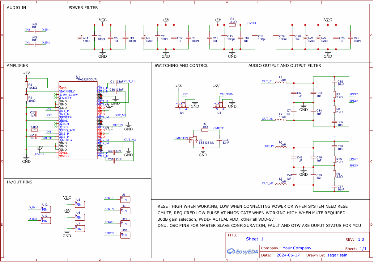
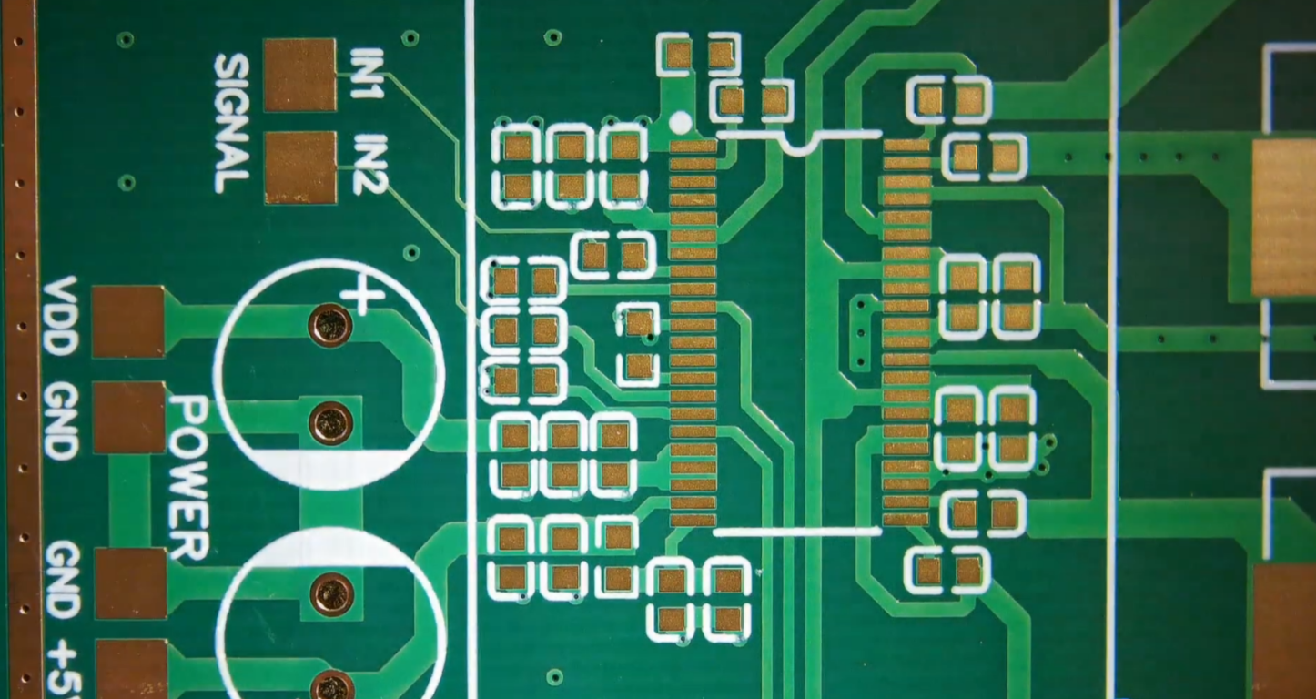
1) Audio Input:
The input stage is straightforward. I used single-ended inputs (IN1, IN2) through 1uF AC coupling capacitors (C19, C20). These block any DC offset from the source and pass only the audio signal. The positive input pins (IN1_P, IN2_P) receive the signal. The negative inputs (IN1_M, IN2_M) are tied to AC ground through their own coupling caps. This sets up the single-ended input mode as described in the datasheet.
2) Power Filtering:
This is where I spent the most time. A Class-D amplifier switching at 600 kHz is essentially a high-frequency power converter, and the power supply decoupling has to be right or you will hear it. The main PVDD rail (7 to 30V) gets filtered with two 470uF electrolytic bulk caps (C14, C29) plus 100nF and 1uF ceramic caps placed close to the PVDD pins. For the 5V rail, I made a deliberate choice. I bypassed the internal LDO and used an external 5V supply. The TPA3221 has a built-in LDO, but for a high-power design, I prefer having a dedicated 5V source. This keeps the analog supply clean and avoids loading the internal regulator.
3) Amplifier Configuration:
The TPA3221 is configured in stereo BTL mode (2 x BTL). Gain is set to 30 dB by the resistor divider on the GAIN/SLV pin. R5 (100k) pulls to +5V and R4 (39k) pulls to GND. 2. R3 (51k) on the FREQ_ADJ pin to GND sets the nominal PWM frequency to 600kHz. The HEAD pin is left floating, which defaults to AD (amplitude-defined) modulation. AD mode gives lower idle current and better efficiency at low output levels. C1, C30, C31, C32 is 33nF on each BST pin pair. These charge during the low-side on-time and provide the gate drive voltage for the high-side MOSFETs.
4) Reset and Mute Control:
The RESET pin needs to be held HIGH during normal operation. When you first connect power, you pull it LOW momentarily to initialize the chip, then release it HIGH. I brought this out to a pin header (U4) for manual control. The CMUTE pin requires a LOW pulse to unmute the amplifier. When CMUTE is HIGH, the outputs are muted.
5) Output Filter:
Each half-bridge output gets an LC low-pass filter, a 10uH inductor followed by filtering capacitors. This reconstructs the audio waveform from the PWM switching signal. The snubber networks are important and often overlooked in DIY designs. I placed a 2.2-ohm resistor in series with a 1nF capacitor (R7-R10, C33-C34, C39-C40) on each output. These damp the ringing caused by the inductor-capacitor resonance and the parasitic inductance of the speaker wires. Additional 10nF caps (C35--C38) sit across the differential outputs, and 1uF caps (C6, C7, C41, C42) provide further filtering.
Key Components:
- U1 (TPA3221DDVR) | 100W Class-D amplifier IC
- C14, C29 | 470uF electrolytic | Bulk decoupling, PVDD
- C19, C20 | 1uF ceramic | Input AC coupling
- C1, C30, C31, C32 | 33nF ceramic | Bootstrap capacitors
- L1, L2, L3, L4 | 10uH | Output LC filter inductors
- R7, R8, R9, R10 | 2.2 ohm | Output snubber resistors
- C33, C34, C39, C40 | 1nF | Output snubber caps
- R3 | 51k | Switching frequency (600 kHz)
- R4 | 39k | Gain select (30 dB) to GND
- R5 | 100k | Gain select (30 dB) to +5V
- R1 | 2.2 ohm | AVDD/GVDD RC filter
- U2 (BSS138) | CMUTE control MOSFET
- C23 | 33nF | CMUTE timing capacitor
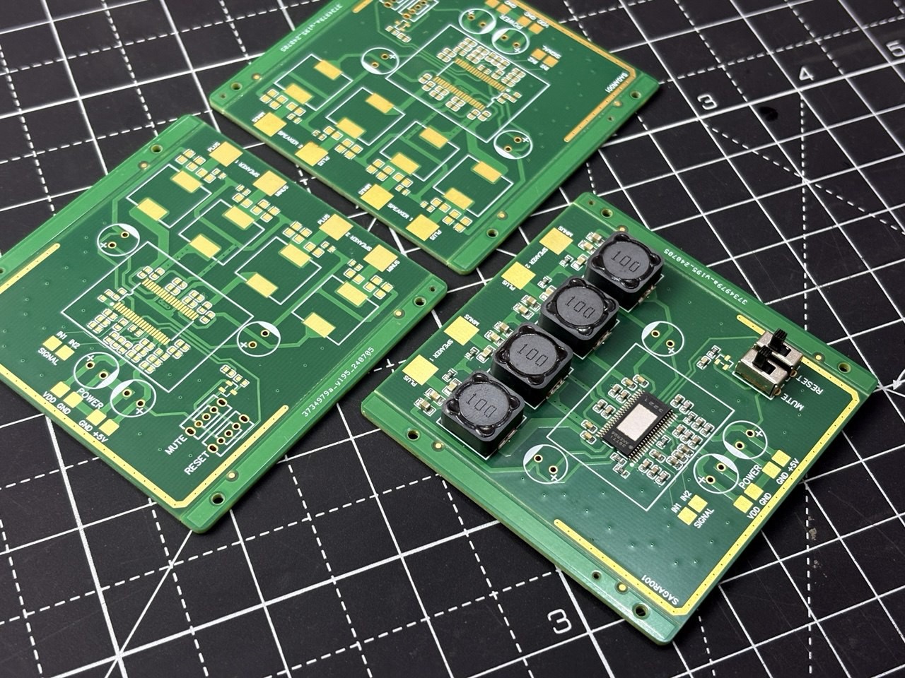
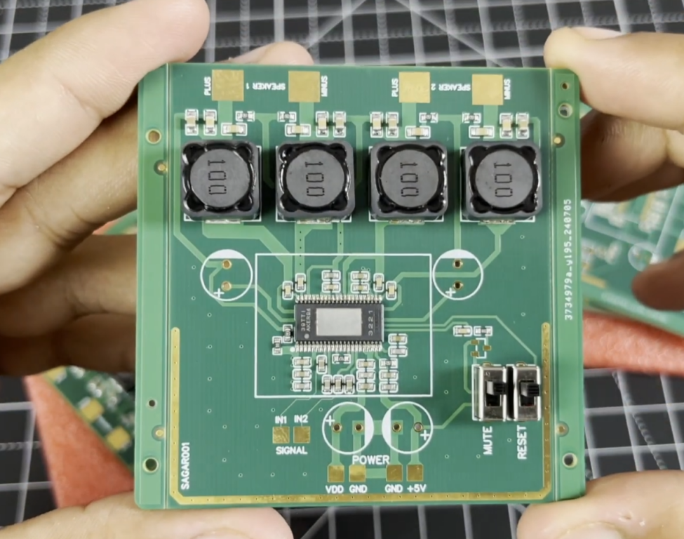
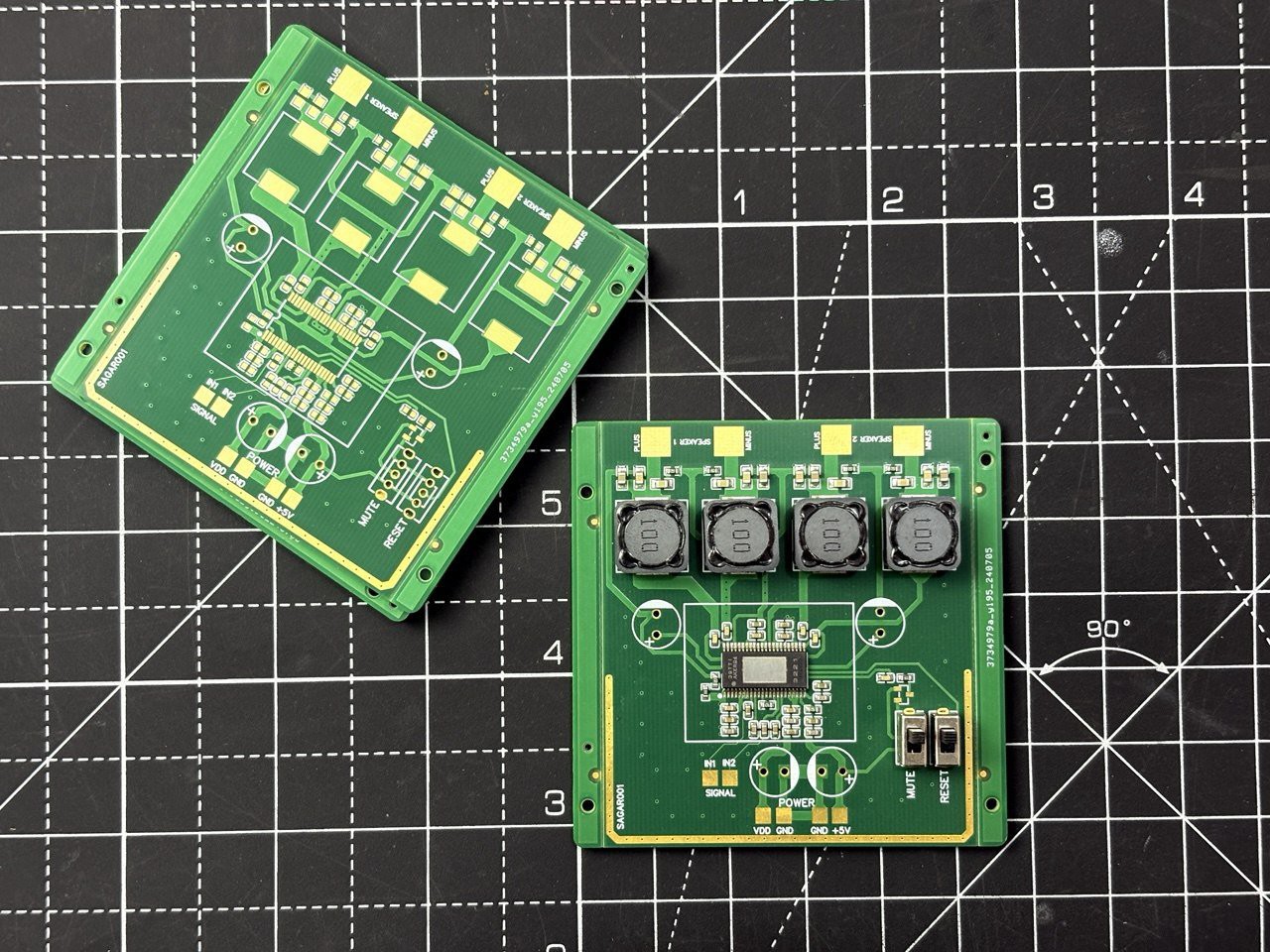
PCB Design:
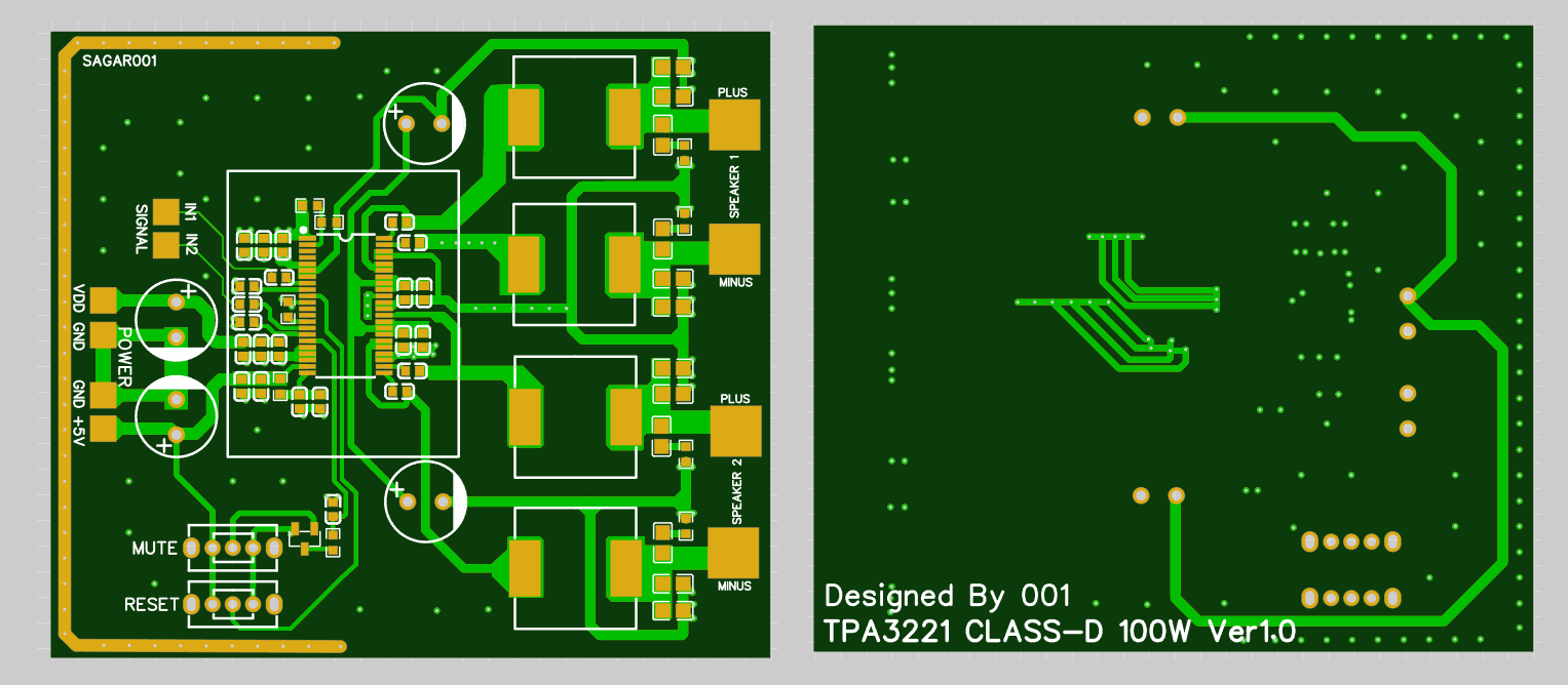
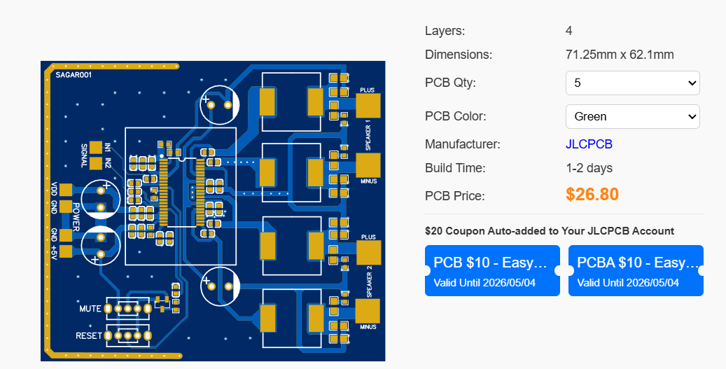
This is a 4-layer board designed in EasyEDA. The dimensions came out to 71.25mm x 62.1mm which is compact for a 100W stereo amplifier. I have used the top and bottom layer for signal and internal layer as references. Layer 2 for ground plane and layer 3 for power plane. Then pour the copper fills on the top and bottom to reduce any crosstalk. I used the services from JLCPCB in order to build this board, and I am amazed by the assembly services the board came to me is perfect and ready to use, You can try JLCPCB for your projects.
The TPA3221 sits at the center of the board. On the left side the audio input connectors (IN1, IN2 signal header) and power connectors (VDD, GND, +5V) are placed. Right side is for speaker output connectors (Speaker 1 and Speaker 2, each with PLUS/MINUS pads). In the bottom left MUTE and RESET pin headers with a switch is placed for manual control. The two 470uF electrolytic caps are placed one near the power input and one near the output stage. This distributes the bulk capacitance where it is needed most. Download all the design files from here.
Thermal Pad Handling:
Here in the IC thermal pad is on the top of the IC, not at the bottom. Most power ICs have a bottom-side exposed pad that you solder directly to the PCB and connect to a ground plane with thermal vias. With the TPA3221, the top-side thermal pad is designed to interface with a heatsink mounted on top of the chip. The datasheet recommends a junction-to-ambient thermal resistance of 44.8 degrees C/W without a heatsink and 5.5 degrees C/W with a fixed 85 degrees C heatsink.
Testing and Results:
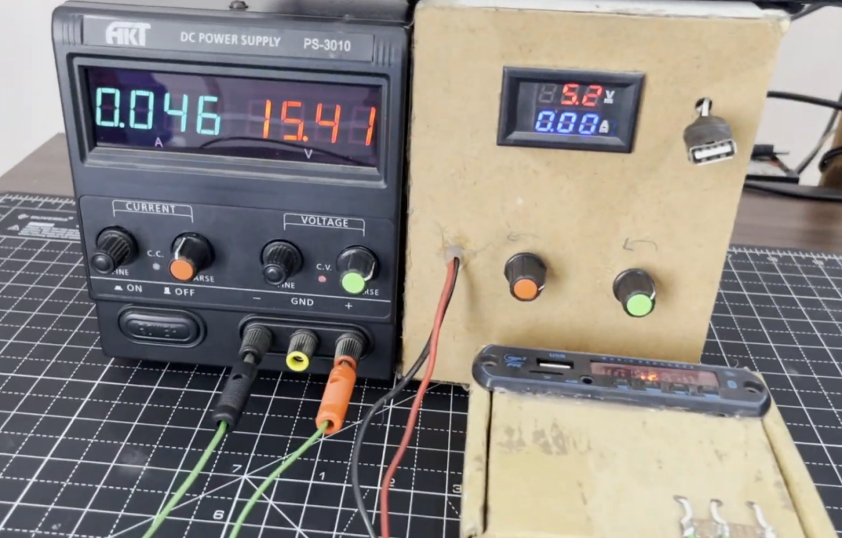
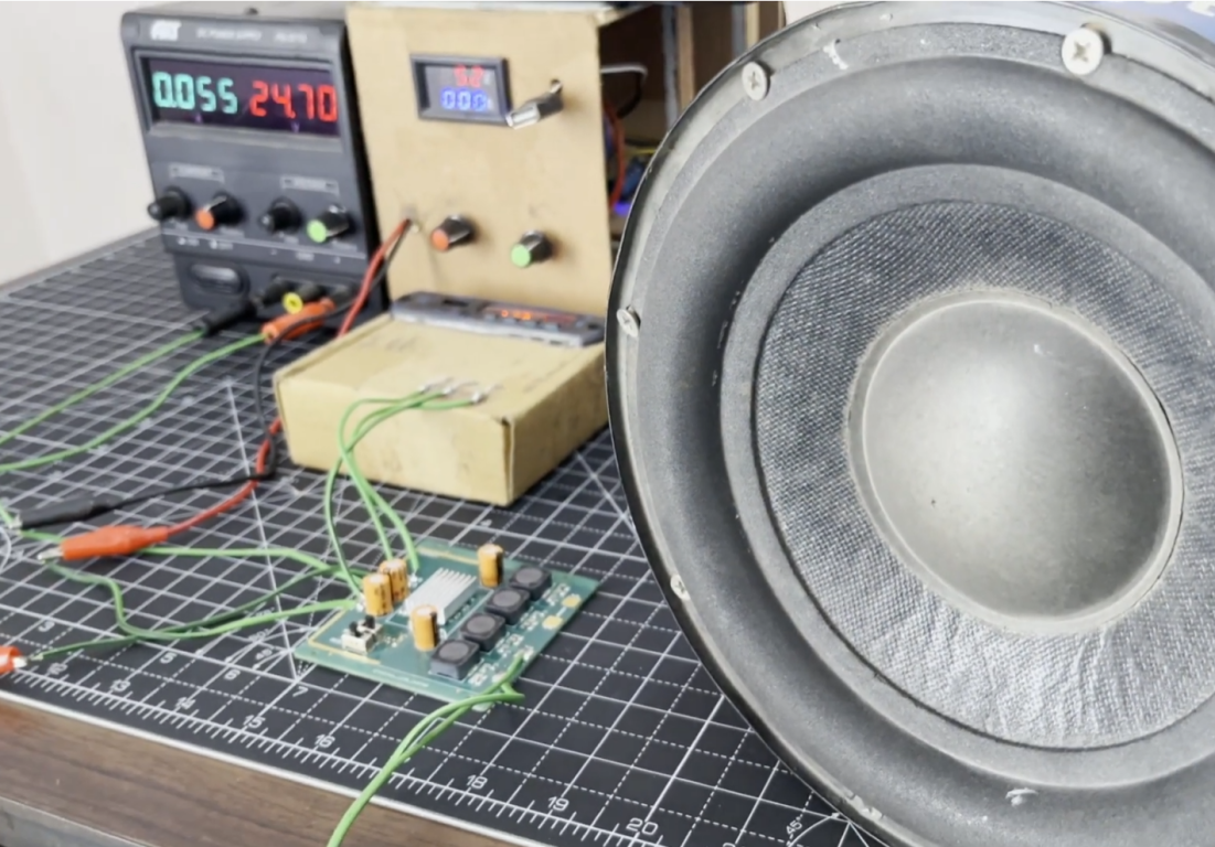
I powered the board with a 24V bench supply and an external 5V for the logic rail with another power supply to monitor the current in both. After the initial reset sequence (pull RESET low, then high) and unmuting via the CMUTE header, the amplifier came alive. For the full audio test you can refer to the video attached here.
I have tried music playback, frequency sweep, bass response, and real listening impressions with actual speakers. Audio quality is one of those things that does not translate well to text. You need to hear it. What I can say here at moderate listening levels, the amplifier is dead silent. No hiss, no hum, no audible switching noise. The closed-loop feedback does its job and the sound is noticeably cleaner than open-loop Class-D designs I have tried before.
Outro:
The TPA3221 is a seriously capable Class-D amplifier IC. For a single chip with minimal external components, getting 100W stereo with 0.02% THD+N and >108 dB SNR is impressive. All the design files are shared with this project. If you build one, I would love to see it.