• Streaming Data Over USB

    Paul Horsfall2 hours ago 0 comments

    My goal for this project is to build a (somewhat) general purpose data acquisition device that's capable of digitising two analog inputs and streaming the resulting samples to a PC over USB.

    I now have a basic first-pass of this working. The main limitation at the moment is that it only streams a single channel.

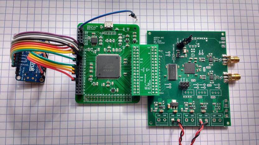
    On the hardware side I'm using a FT232H USB bridge and a Lattice iCE40 FPGA. The FT232H makes it easy to talk USB, while the FPGA interfaces between the USB bridge and the ADC.

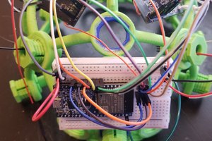
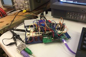
    Here's a picture of the set-up:

    The ADC I'm using has a resolution of 10 bits and I'm running it at 8 MHz. If I use two bytes per sample, then for two channels, I'll need to push 32 MB/s over USB. To achieve this with the FT232H it must be configured in synchronous FIFO mode. In this mode, the FT232H generates its own 60 MHz clock to pace data transfers.

    Since the FPGA sits between the ADC, which is driven by an 8 MHz clock, and the FT232H, which is driven by its internal 60 MHz clock, it has to handle cross domain clocking. The standard way to achieve this is with an asynchronous FIFO, and for that I'm using this library.

    On the PC side, I'm using libFTDI to talk to the FT232H. I've written a very simple program to forward data from the device to stdout. The output from this can then be redirected to a file, or piped to another program for processing, visualisation, etc. The implementation is more-or-less just a thin wrapper around ftdi_readstream.

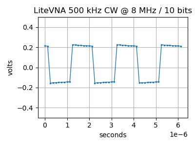
    Here's a plot showing data captured using this set-up. In this example the input was driven by my LiteVNA in CW mode at 500 kHz.

  • Assembled ADC Breakout Board

    Paul Horsfall05/06/2026 at 15:45 0 comments

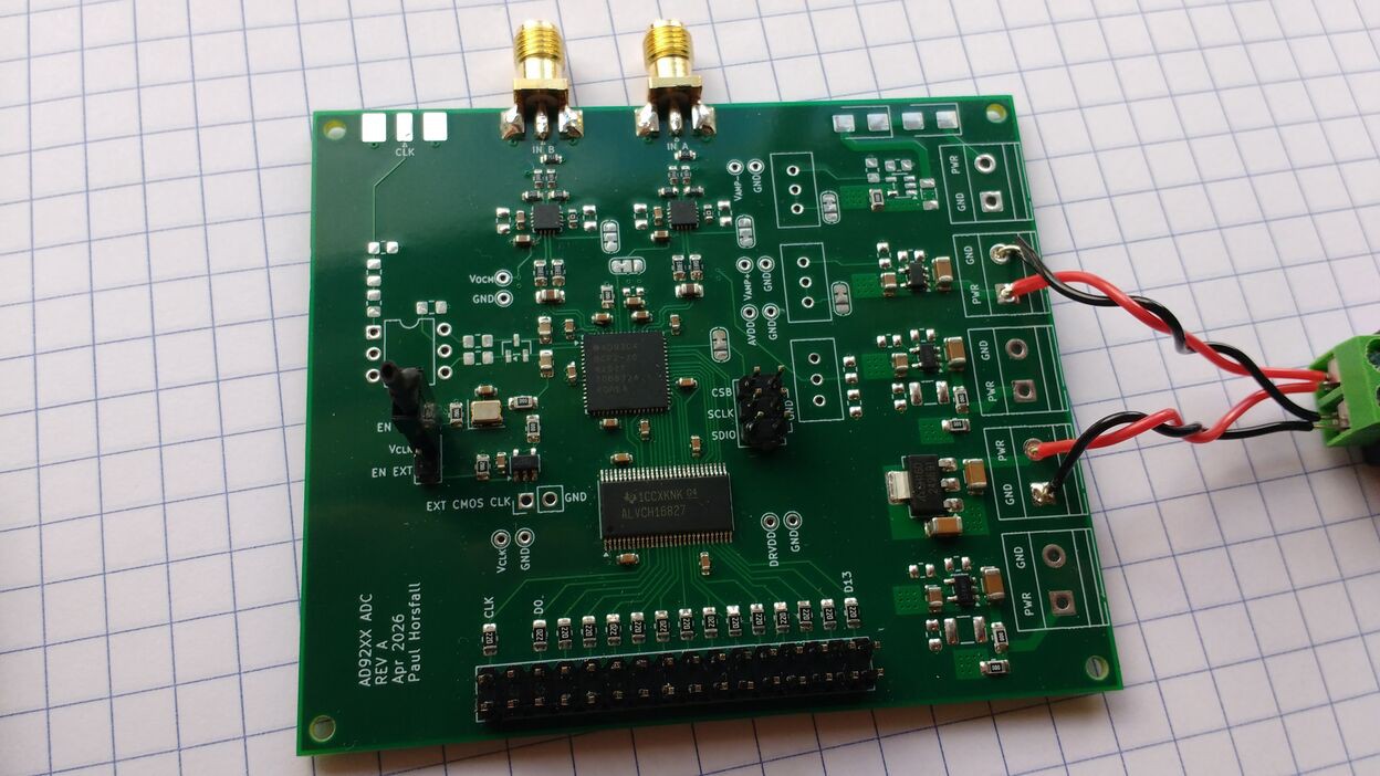
    Here's a picture of my first attempt at assembling one of my ADC breakout boards:

    I used the hotplate method for the surface mount parts, and then hand soldered the through hole parts and SMA connectors with an iron.

    This instance is populated with an AD9204 for the ADC, an 8 MHz crystal oscillator for the clock, and a pair of ADA4940 amplifiers configured for a gain of two and 50 ohm input impedance.

    I've already performed a few basic checks to determine whether the board is working as expected:

    • The DC voltages on the power rails look good.
    • The oscillator is running.
    • The ADC clock output looks good.
    • I'm seeing switching on (at least some of) the data outputs.
    • The input impedance of both inputs looks like 50 ohms. (This suggests the amplifiers are working.)

    So far so good. The next step is to attempt to read the data coming from the ADC.

  • ADC Breakout Board

    Paul Horsfall04/29/2026 at 15:39 0 comments

    As mentioned in the introduction, I've been working on a breakout PCB to facilitate experimenting with the family of ADCs I'm considering using for this project. The board supports the 10 bit / 20 Msps AD9204 that I expect I'll use initially, but can also work with a range of pin-compatible parts, which I may use to experiment with 12 or 14 bit parts.

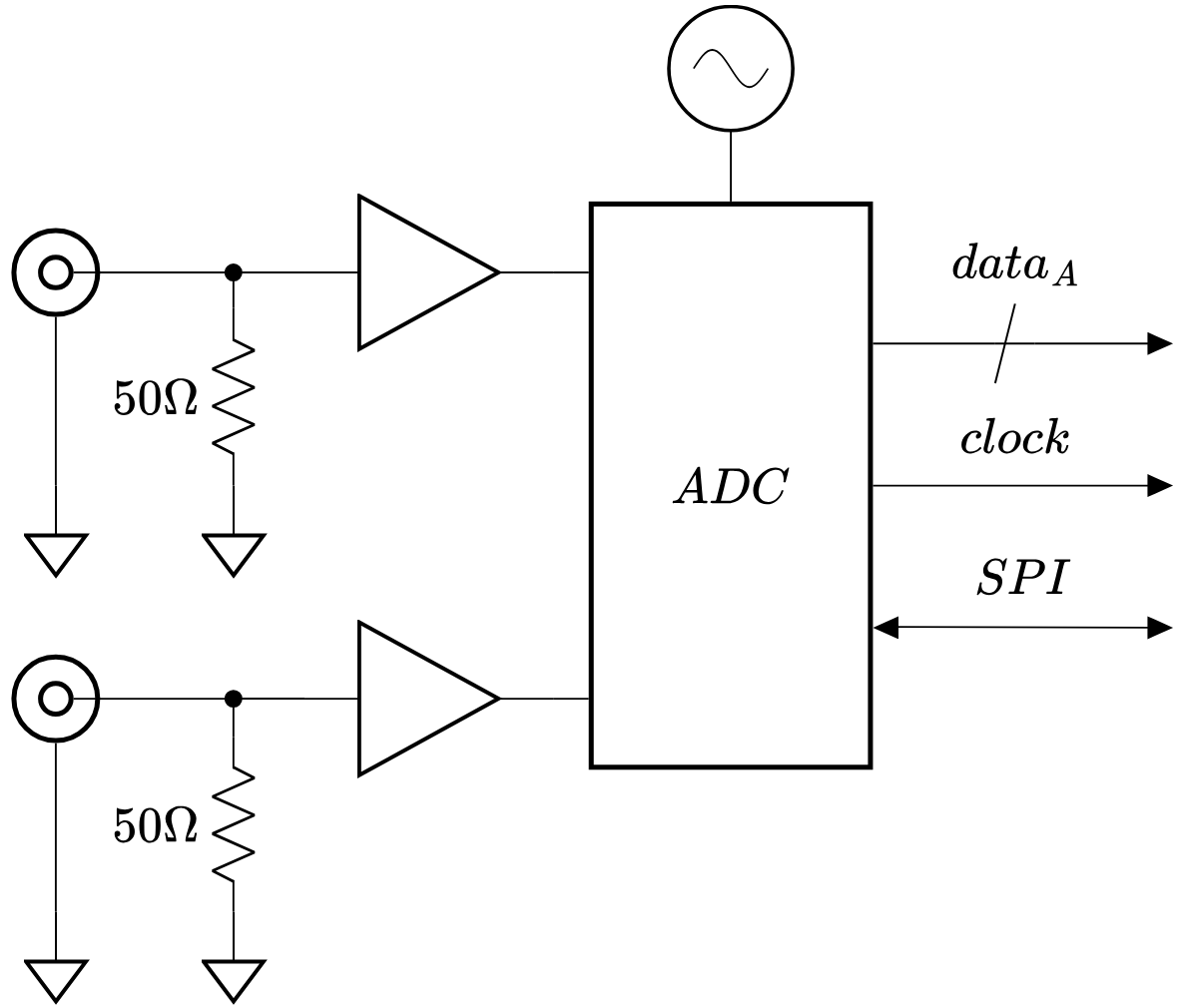
    Here's a diagram that gives a high-level view of the design:

    There are two 50 ohm inputs, each driving one of the two ADC inputs through a buffer. A crystal oscillator provides a low jitter clock to drive the ADC. (Though not shown in the diagram, I also have a couple of options for driving the ADC from an external clock.) One of the ADC's two data and clock outputs is made available via pin headers. (I choose to expose only a single output channel because I couldn't conveniently connect both channels to my FPGA breakout board. However, the ADC is capable of multiplexing both channels onto a single output, so I expect to still be able to make use of both channels.) The ADC's SPI interface is also available on pin headers.

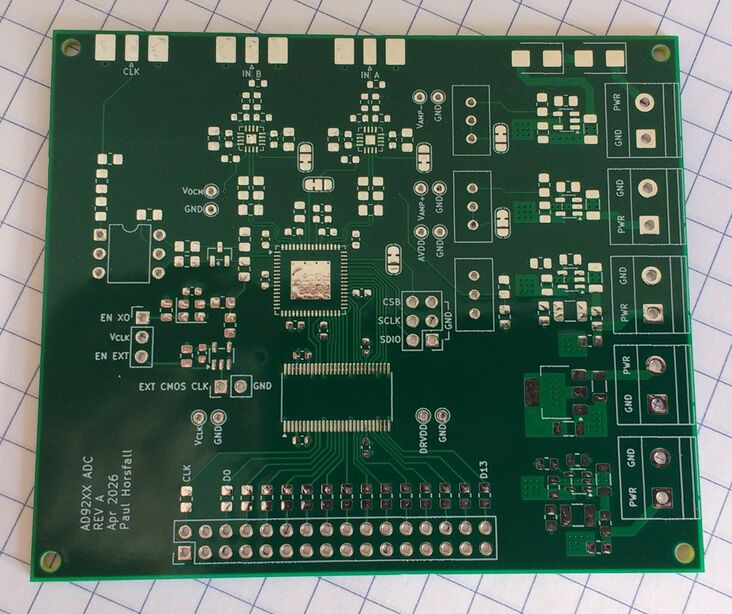
    The board was laid out in KiCAD and manufactured by JLCPCB. Here's a picture of an unpopulated board:

    The next step is to attempt assembly...

  • Introduction

    Paul Horsfall04/29/2026 at 10:15 0 comments

    With this project I'm aiming to build a data acquisition device with the following rough specs:

    • 2 analog channels
    • 10-12 bits
    • ~8 Msps (perhaps faster at 8 bits, or when running a single channel)
    • Coax connectors (SMA or BNC)
    • USB 2

    My high-level plan is to build this around a Lattice FPGA (so I can use yosys, nextpnr, etc.), a FT232H USB bridge, with something like an AD9204 for the ADC.

    I'm not sure what I want from the front-end yet (input impedance, bandwidth, gain etc.) but I'll figure that out as I go.

    I'll start by experimenting with breakout boards. I already have these for the FPGA and USB bridge, and I've started work on a custom break-out board for the ADC.

    My hope is to eventually use this to upgrade the data acquisition stage of my homebrew SDR receiver. I can also imagine this being useful as a general baseband / IF digitizer for other projects I have in mind.