 Edward Viaene
Still working on the v2 version. Currently doing component placement, which means that (hopefully) the schematics are not going to change much anymore. What analog looks like right now:
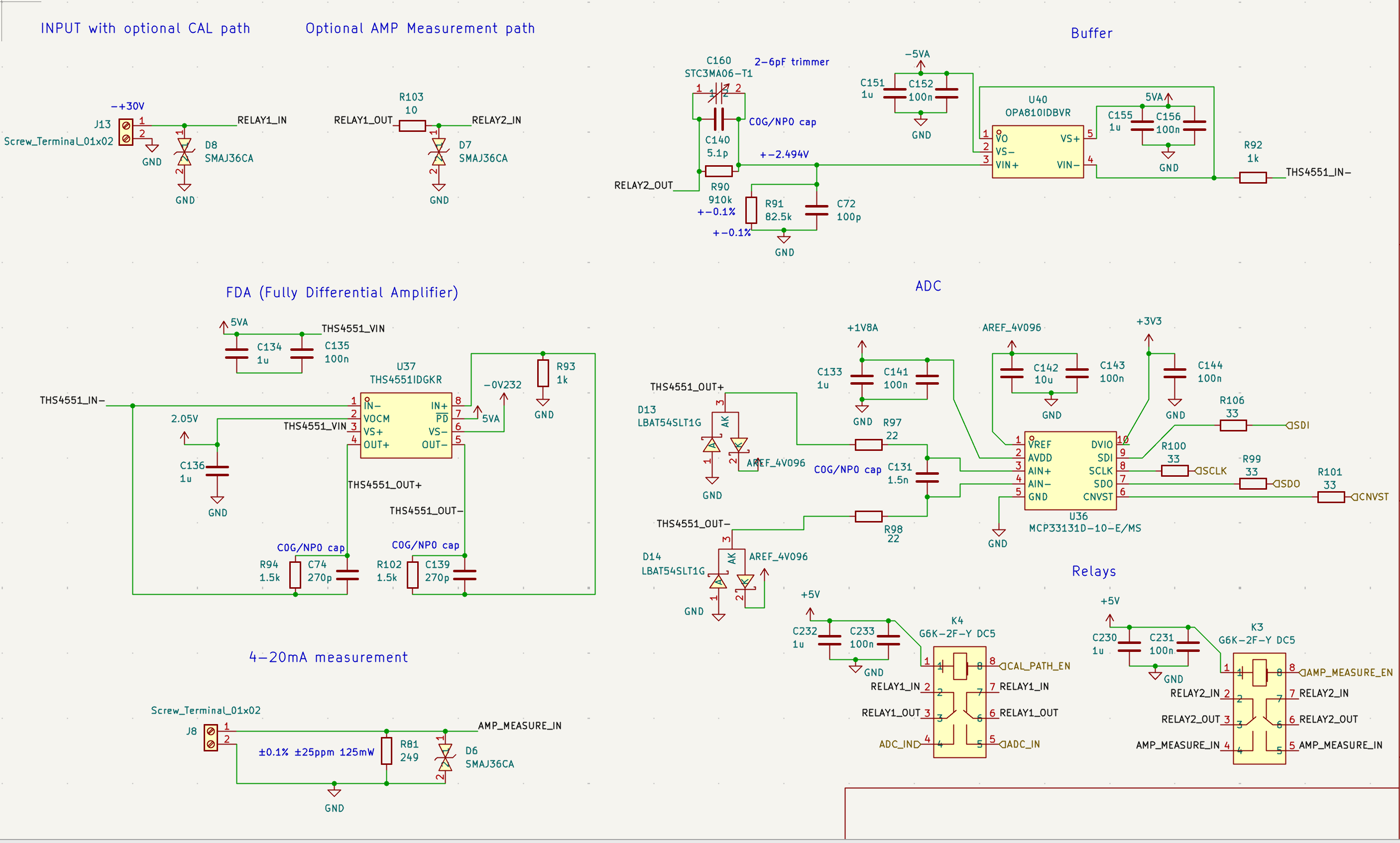
- ADC: +-30V input, OPA810 buffer, THS4551 Fully Differential Amplifier, and MCP33131D-10 as ADC (1MSPS, 16 bit). That is ~400 kHz usable signal bandwidth
- A 4-20mA measurement path can be switched with a G6K-2F-Y relay. It'll connect before the 12:1 divider and reuse the same ADC
- For calibration, there's also another G6K-2F-Y relay that can disconnect the input path and connect the DAC so that we can calibrate the DAC to ADC path
Here's the ADC schematic:
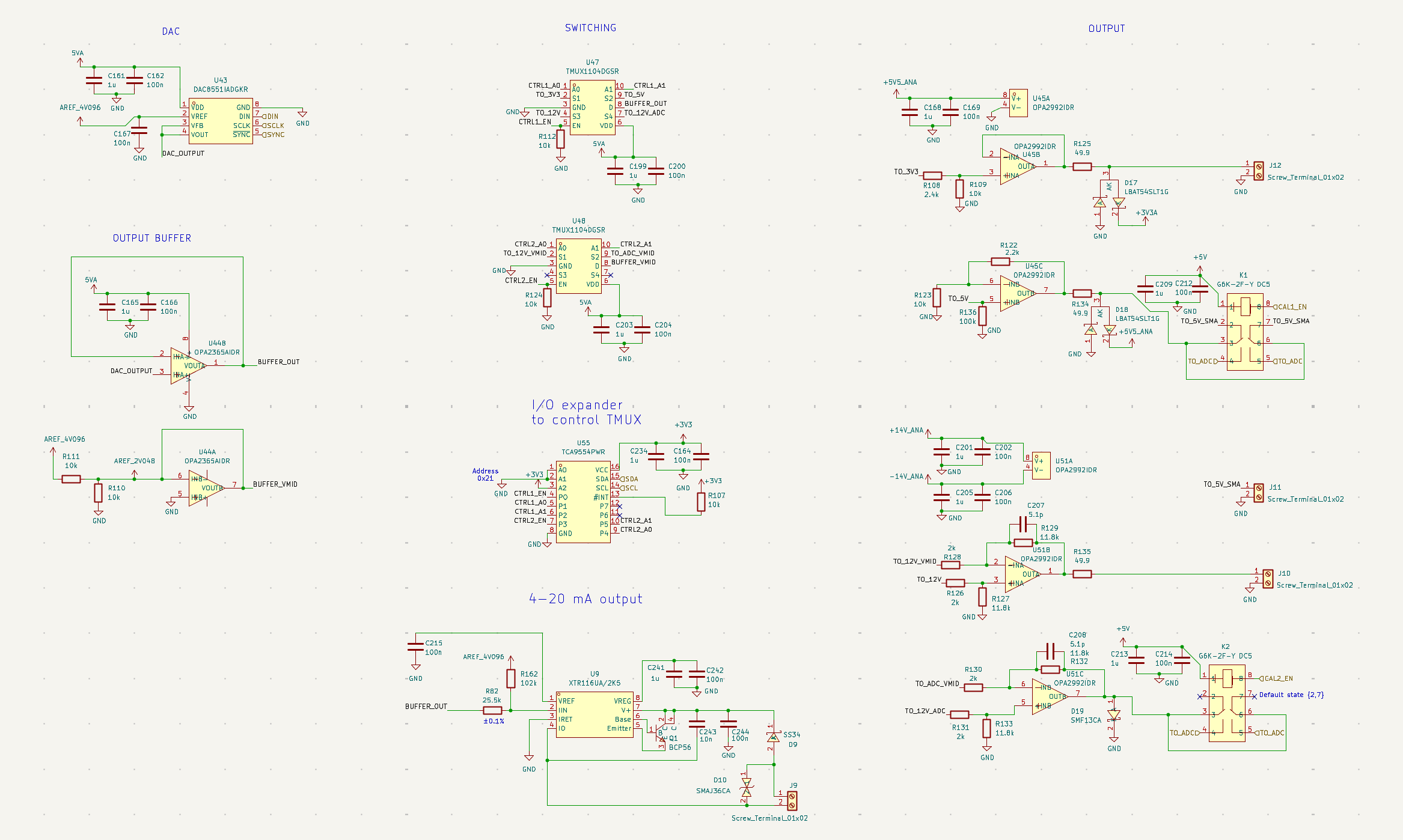
The DAC is a 16 bit DAC8551 with an OPA2365 buffer. I have a few TMUX1104 that can switch the path to different voltages: 0-5V, 0-3V, and -+14V. The -+14V is the path that can output to the ADC for calibration.
There's also a 4-20mA output from the DAC. There's another relay that can switch between outputting to the regular path or to the 4-20mA output path.
The DAC schematic:
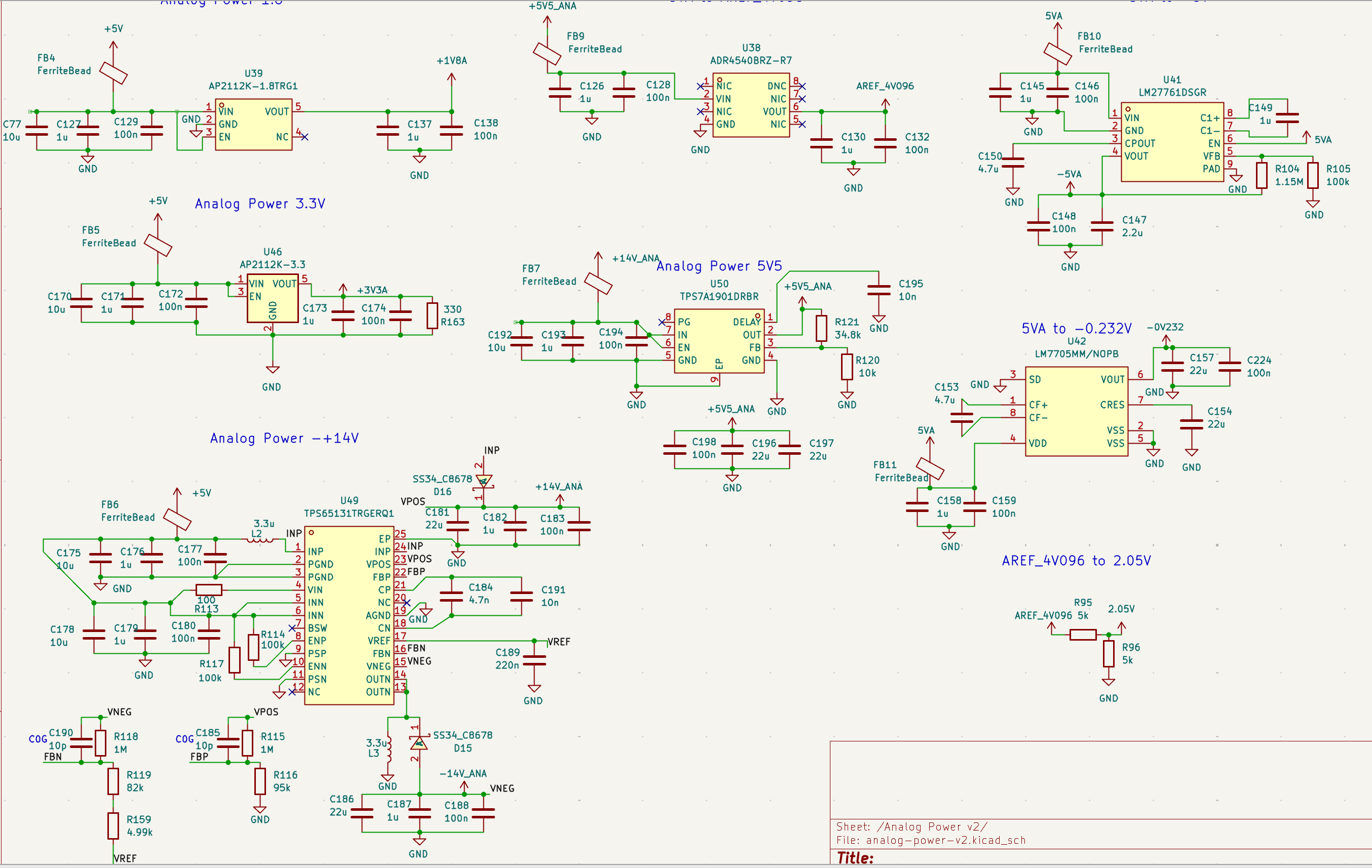
Lots of parts, which means lots of loader fees at JLC, so let's hope it doesn't need many respins! There are 8 different voltages to work with in the analog section:
Discussions
Become a Hackaday.io Member
Create an account to leave a comment. Already have an account? Log In.