 Edward Viaene
Finalized v2.0.0 and ordered it on JLCPCB (the new schematic is under files). A few notes
- PCBA standard is needed for ESP32, I knew that from the v1 version, but when you have more components, at some point the benefit of PCBA economy will disappear once you have a lot of extended components. This is because it's 3 USD per extended component in economy, but 1.5 in standard
- The RGB LED I picked needs some special treatment, which is another ~10 USD on top of that, and also bumps you out of PCBA economy
- The combination of lots of extended components and the ESP32 (for WiFi) makes, in my case PCBA standard roughly the same price (it's perhaps 10 USD difference)
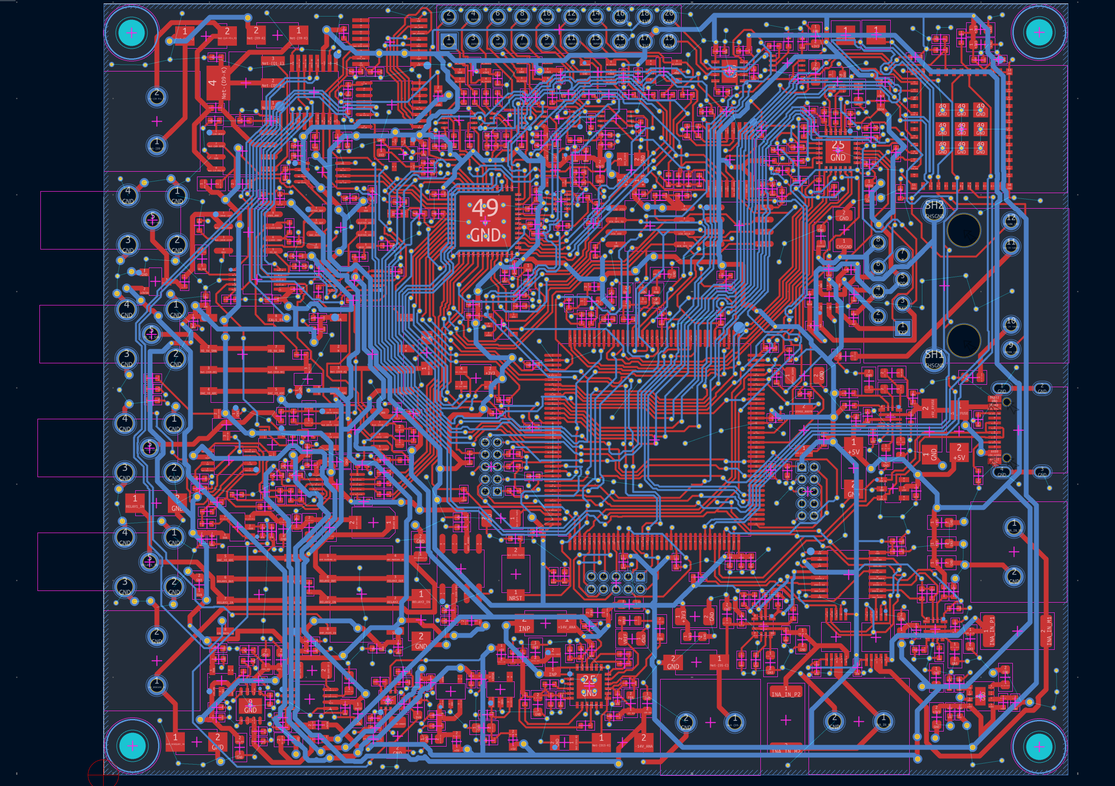
There are lots of components in v2.0.0, but the board size is the same. On multiple occasions, I wondered about expanding the board or going to more layers. More layers are much more expensive, so a bigger board would be a better solution. Still managed to route everything with the same board size. Almost all the analog path is routed on top. The power at the bottom. For the digital path, it's more mixed, but that should be OK. Here's a screenshot of the wired PCB. Left is analog, middle and right is digital. I removed the ground fill to make it more readable.
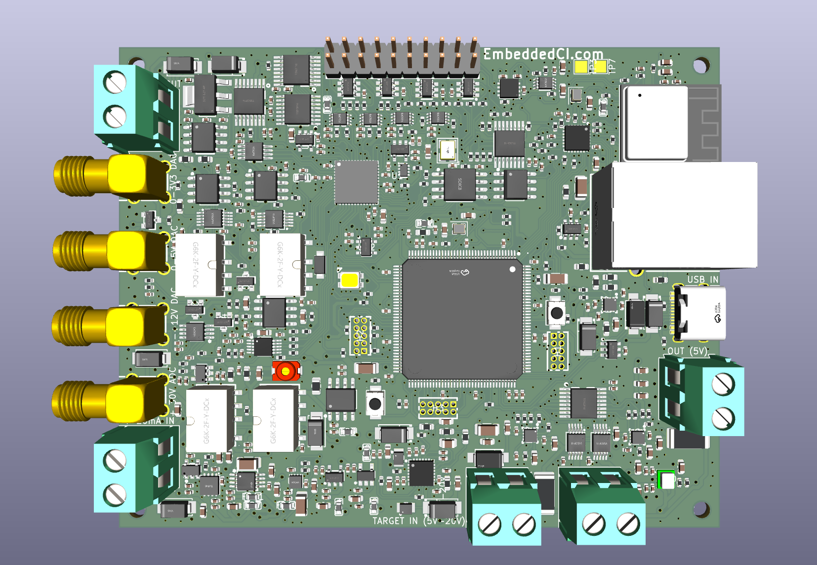
Here's the 3D overview. I picked SMA for the analog path (ADC / DAC) and screw terminals for the 4-20mA measurement and output. And yes, this STM32 is huge.
The difficulty with wiring the STM32H563 is that the pins are scattered across multiple protocols. RMII is on all sides, SPI is on all sides, so there's no perfect orientation for the chip. That quickly translates into trying to get all these traces from the ESP32 and RMII down to the STM32 and wiring it up from there.
Discussions
Become a Hackaday.io Member
Create an account to leave a comment. Already have an account? Log In.