 Geert Roumen
Modern development boards are more advanced than ever. Yet identifying the correct pin can still be surprisingly difficult.
A microcontroller is inherently complex. Finding the correct GPIO pin shouldn’t be.
Engineers already use visual design principles everywhere. It seems that it is often not applied to PCBs.
PCB silkscreen is often treated as a purely technical artefact rather than a communication medium. In both cases, usability work is frequently seen as secondary to the “real” engineering. We need more focus on the User Experience (or Developer Experience) to make things better for everyone, including beginner and expert developers. This is not necessarily a trade-of, it can be better for beginners and experts even just by spending a bit more time on designing and testing a pcb without necessarily increasing hardware cost.
1. Make space for information
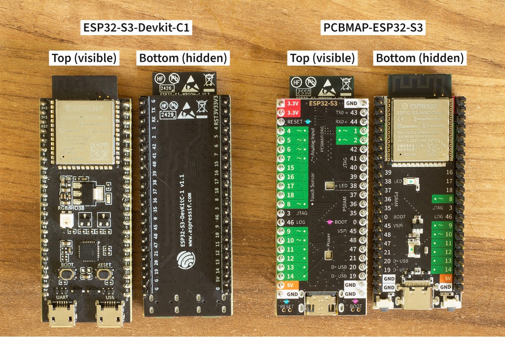
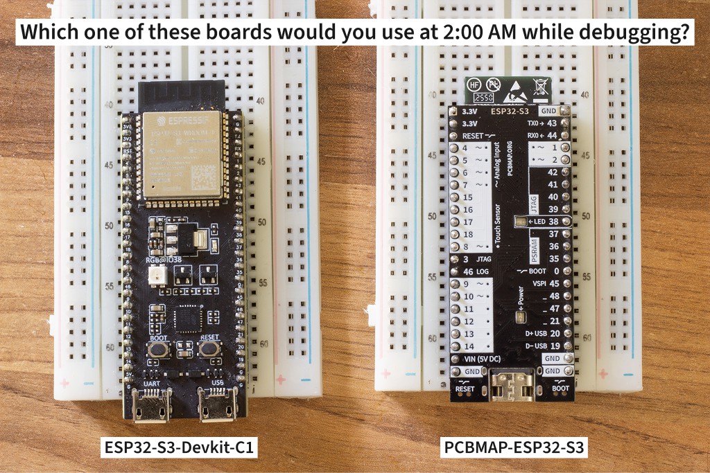
Since the silkscreen is the user interface, we should give space to this. In most dev kits the components are all on the top of the PCB. This is almost like putting the screen of a laptop on the bottom of the laptop; so you constantly have to flip the device or use an external monitor. Some components like pushbuttons, LEDs and jumpers could mounted reversed or on the side to avoid having to solder components on both sides (which costs a bit more and takes up more space on the top side).
All elements are soldered on the bottom side; giving the top side a flat appearance and room for graphics. This could be done by reverse-soldering the LEDS, applying a laminated board type of USB-C connector. It also meant that basically all the connections of the ESP32-S3 module needed to be reversed on the PCB which adds a bit of length and crosstalk to the lines. The buttons (for BOOT and RESET are now sticking out on the USB side; so they can be pressed when the board is on a breadboard. The user LED is placed next to the pin triggering it; also showing this form follows function concept.
2. Create visual hierarchy
The GND and VCC are shown with the boldest font. This should warn the user about using this pins; but also make it easy to find. On the coloured version the GND and VCC are also shown in black/white and red or orange to indicate the different voltages.
The green pins (or white background pins) are the ones you should use first; they don’t connect to anything else and have full functions. Analog inputs and touch sensing pins are marked. Good to note that some green pins that are not marked as analog inputs also could function as analog inputs, but only when the wifi is not used. Since the ESP32-S3 is mostly used as a WiFi-enabled board I choose to not mention this to avoid confusion and these pins can still be used for digital in and outputs or touch sensing.
The pins that are more risky to use, since they have behaviour during boot or are connected to components, are the third layer. You don’t want people to connect an LED to the USB D+ pin, since this might make it impossible to update the firmware on the board. I thought about putting warning icons next to it, but it might be better to highlight which pins should be used instead, since it could easily become a overload of warning symbols.
3. Put labels in readable places
Labels are always placed next to the pins on the top side, on the bottom side some of the pins are just not labelled due to the ESP module being in the way. The pin number is never overlapped with a track on the copper layer, some of the other text or labels is. A solution to this would be to move the top layer to one of the middle layers. This will lead to a nice and clean ground plane...
Read more »