Daniel Knezevic
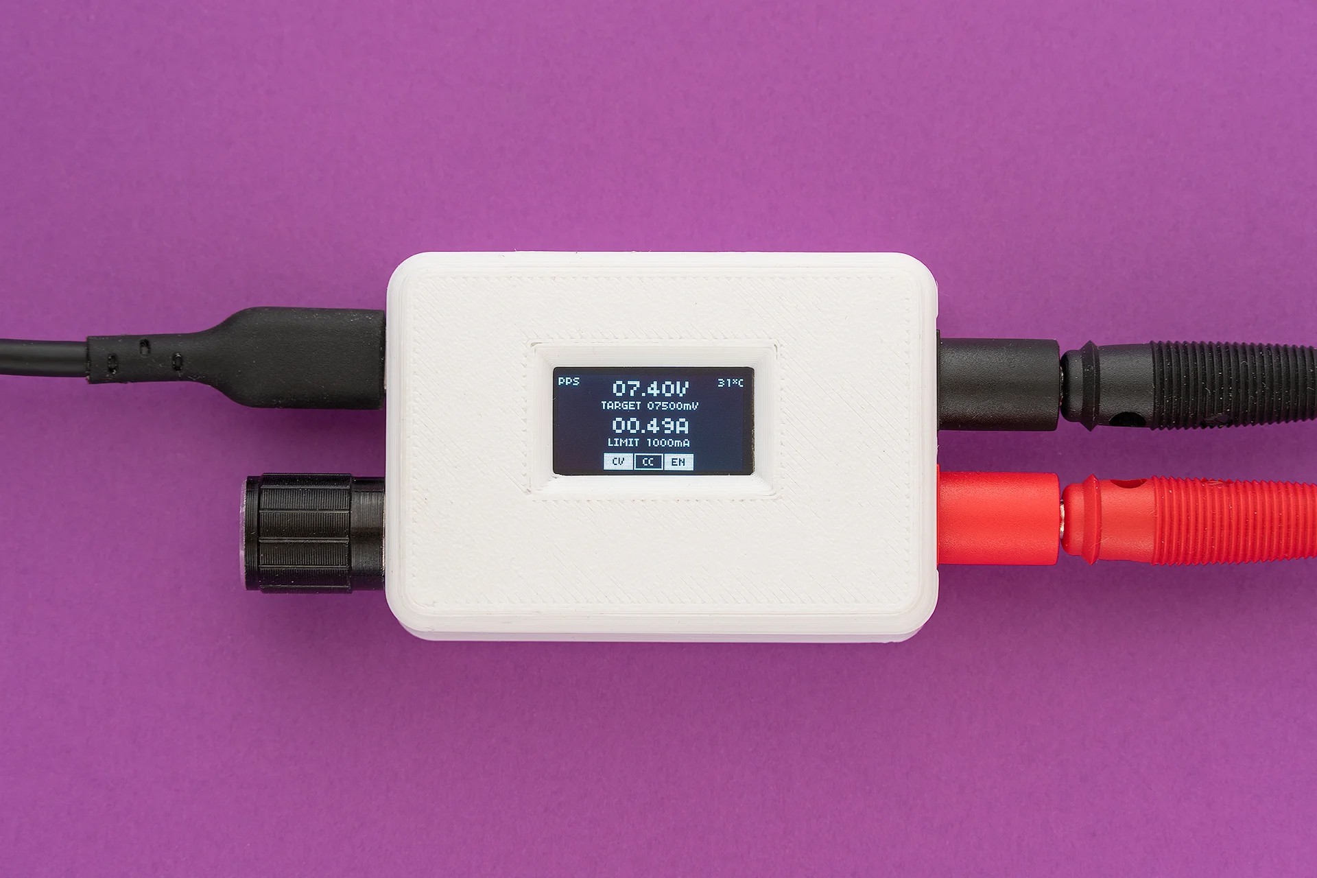
TinyPPS is a pocket-sized programmable power supply built on the USB Power Delivery (PD) standard and the USB Programmable Power Supply (PPS) feature. It transforms a standard USB-C PD charger into a flexible bench-style power source by negotiating selectable output voltages and current limits directly with the charger.
Key features
TinyPPS takes advantage of pin-compatible USB PD sink ICs (AP33772 and AP33772S), providing two feature sets within a single firmware, depending on the selected IC:
| Feature | With AP33772s | With AP33772 |
|---|---|---|
| Supported PDO profiles | fixed PDO, PPS | fixed PDO, PPS |
| Output voltage range | 3.3 - 21V | 3.3 - 21V |
| Max output current* | 5A | 5A |
| PPS voltage step size | 100mV/Step | 20mV/Step |
| Programmable current limit | 250mA/Step | 50mA/Step |
| User-switchable output | ✅ | ✅ |
| Over Voltage Protection (OVP) | ✅ → Hard Reset and Auto Restart | ✅ → Auto Restart |
| Over Current Protection (OCP) | ✅ → Output Disable | ✅ → Auto Restart |
| Under Voltage Protection (UVP) | ✅ → Output Disable | ❌ |
| Over temperature protection (OTP)** | ✅ → Output Disable | ✅ → Output Disable |
| Short-Circuit Protection (SCP) | ✅ → Output Disable | ✅ → Output Disable |
*charger and cable dependent
**OTP is set to 85°C
The idea
Everything started with buying a 15$ USB powered mini SMD hot plate that required a supply with the following capabilities: PD65W 20V 3.25A. By acquiring a 100W power supply I have found out something called PPS, beside regular voltage/current values, on the label.
PPS 3.3V-21.0V - 5.0A 100W max - tickled my brain. What is PPS? It turned out it is a neat USB-C feature. To be more precise, it is an advanced feature of the USB Power Delivery (USB PD) 3.0 standard that allows chargers to dynamically adjust voltage and current in real time. Unlike standard PD, which uses fixed voltage “steps” (e.g., 5V, 9V, 15V, 20V), PPS allows for fine-grained adjustments - typically in 20mV voltage increments and 50mA current steps.
Knowing this, I came up with the idea of using USB PPS to build a small “lab” power supply as a proof of concept. Before jumping in to realisation, I explored existing solutions and stumbled upon PocketPD by Centylab. Inspired by this great project, I came up with an idea to create my own solution and use this opportunity to learn new skills.
Sponsor time
Huge thank you to PCBWay for providing me PCBs and SMD stencil for free.
PCBWay offers high-quality PCBs at affordable prices. The boards are ready to solder straight out of the box, with no leftover tabs that need to be sanded down. Ordering is super easy: just upload the Gerber files and select the desired parameters.
What I like most is their customer support. They are quick to review orders and don’t just point out issues - they provide detailed explanations on how to address them. Whether it is about a missing Gerber file or out of capabilies issue. At the end, the outcome is always positive.
Hardware
For this project I wanted to use a microcontroller family other than ESP32. Options were Raspberry Pico-series or STM32. Due to ease of use (mostly flashing) I have chosen the Pico - RP2040.
The schematic started as an amalgamation of a few reference designs - mostly RP2040, AP33772S and INA226, with an OLED, rotary encoder and some extra connectors added on top.
When I realised the older AP33772 variant provides smaller voltage and current steps for PPS compared to AP33772S I tweaked the schematic to handle both USB PD sink controllers. The good thing is that these two ICs are pin compatible.
Schematic and PCB are designed in KiCAD 10:
Difference between AP33772 and AP33772S
Shunt resistor: AP33772 requires a 10 mΩ shunt resistor while AP33772S requires 5 mΩ.
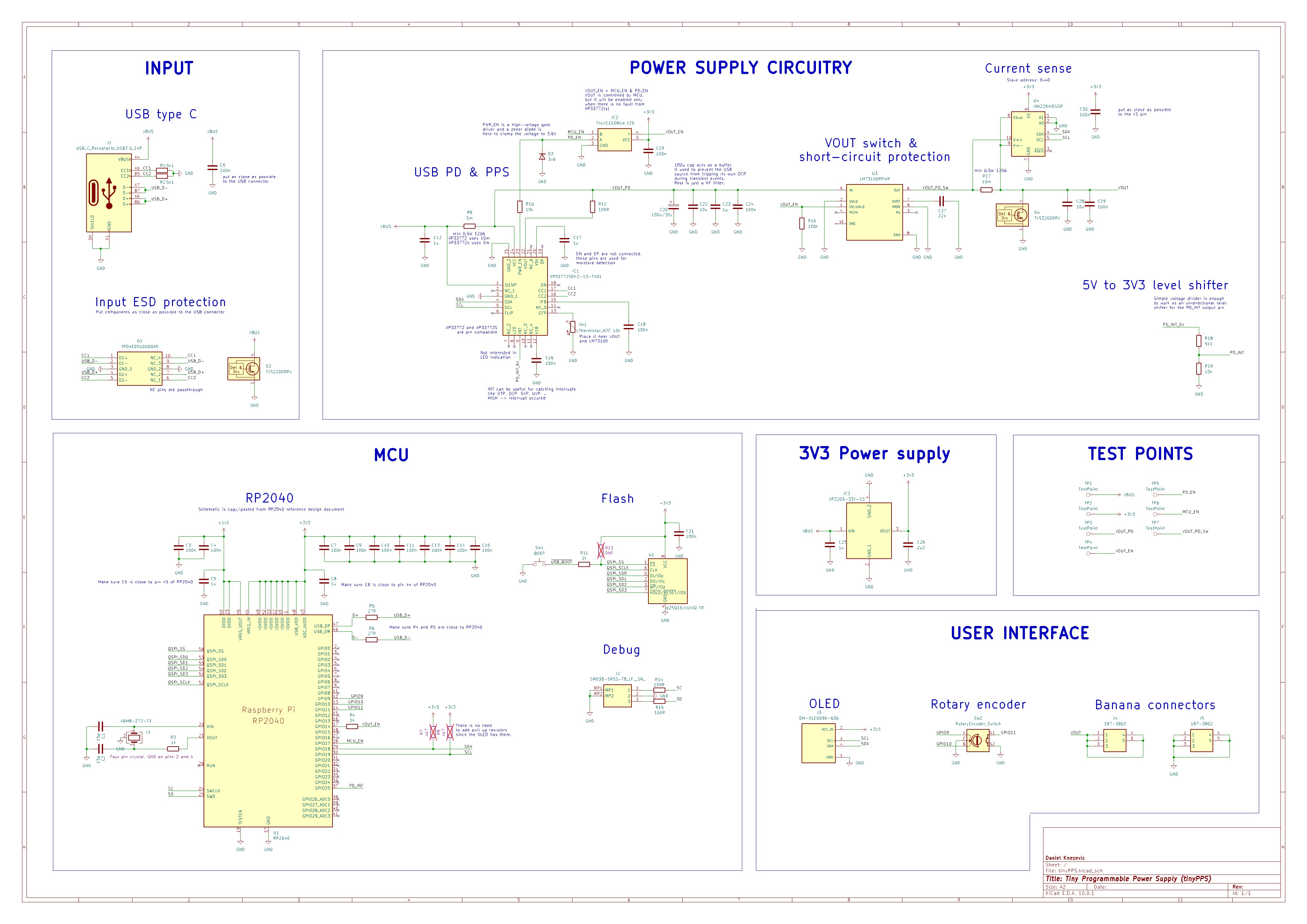
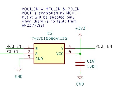
VOUT control: While AP33772S has an option to manually enable/disable the output via the VOUTCTL bit in the SYSTEM register, the AP33772 enables the output automatically upon successful PD negotiation. To support both ICs and have the same feature for manual output handling, an AND gate is added between the AP33772(S) PWR_EN signal and the LM73100 enable pin. The AND gate combines the PWR_EN signal with an RP2040-controlled enable signal, forming the final enable for the LM73100. Another benefit of the AND gate is that the output is disabled by default.
The output (Y) of the AND gate is connected to RP2040 input pin and its value is used in combination with INA226 to handle faults like short-circuit. If the output is enabled but the INA226 reports 0V, it indicates that the LM73100 has shut down, likely due to a short circuit. In this case, the system disables the output.
Note: For AP33772S, it is important to leave VOUTCTL bit unchanged - set to 0.
While reference design of AP33772(S) use a back-to-back NMOS switch for controlling the output, TinyPPS is using an ideal diode (LM73100). The swap is not straight forward cause the PWR_EN signal from AP33772(S) acts as a gate driver and exceeds the LM73100’s absolute maximum voltage rating, so it cannot be connected directly to the enable pin.

Because the PWR_EN voltage scales with the PPS output and remains higher to fully enhance the NMOS, a simple resistor divider is not sufficient. Instead, a 3V6 Zener diode is used to clamp the signal to a safe level.
Using LM73100 introduced short-circuit protection to TinyPPS at a cost of dropping support of AVS profiles for AP33772S. True to its name, TinyPPS supports only PPS voltages (3.3 to 21V) due to LM73100’s maximum operating voltage of 23V.
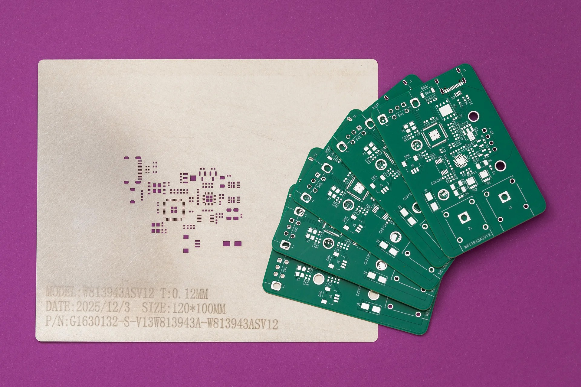
PCB design
This is the first time I designed a PCB with 4 layers. The 4-layer stack-up is arranged as signal, ground, power, signal. The intention was to improve signal integrity by providing a continuous ground reference and reducing noise compared to a 2-layer design.
Besides this, I calculated trace widths for signal lines and USB differential pairs to meet target impedances based on the stack-up and improved decoupling capacitor placement.
Firmware
Firmware is organized in the following logical layers and modules:
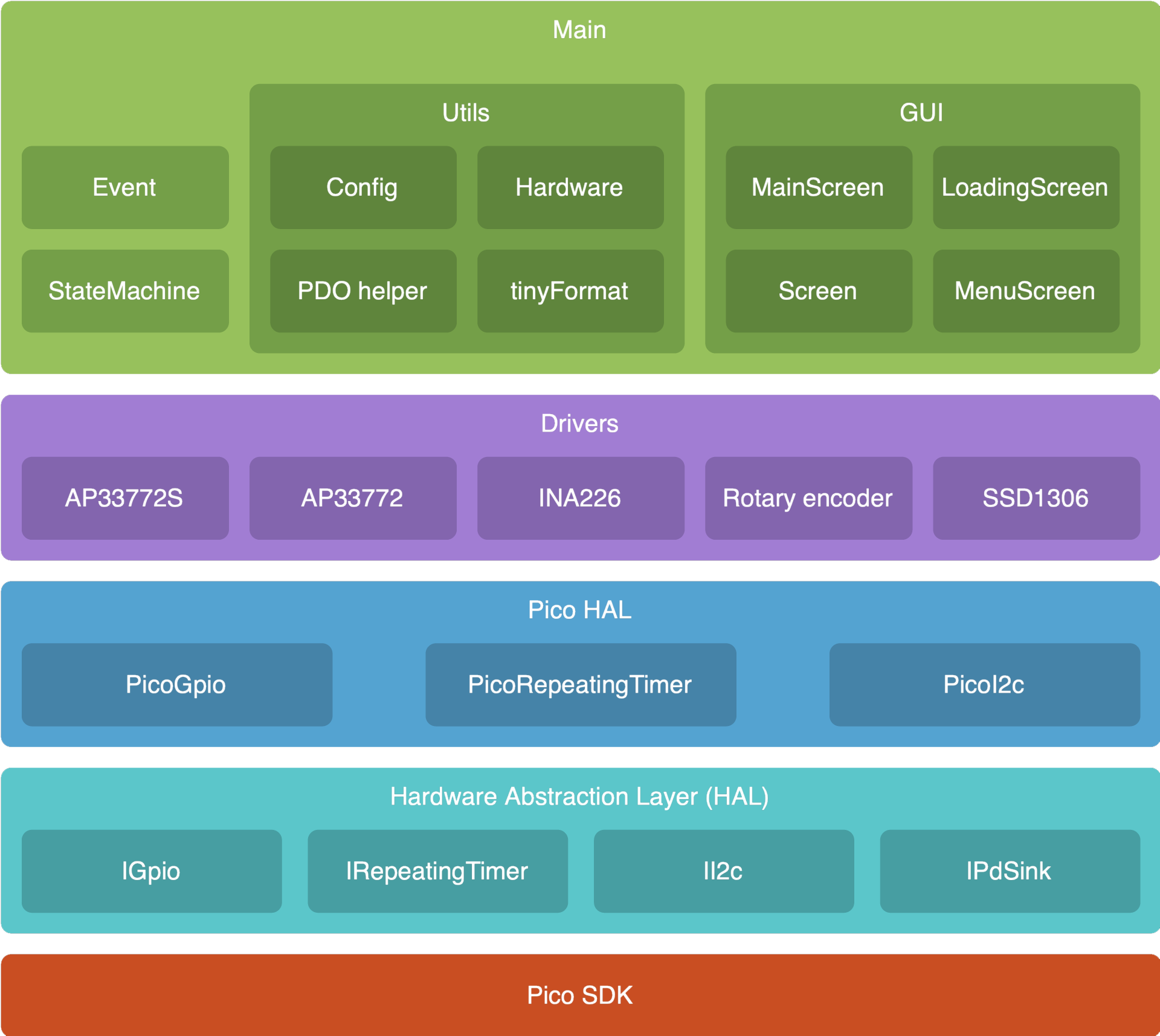
Pico SDK
The firmware is written in C++ (C++20) using the Pico SDK, running directly on the hardware without RTOS.
Hardware Abstraction Layer (HAL)
HAL is created as a set of hardware independent interfaces for controlling microcontroller peripherals like: GPIO, timer and I2C. It provides APIs that other components can use without knowing hardware details. While this layer is not actually needed for this project, since it is running only on RP2040, the drivers for INA226, SSD1306, … can be re-used on other projects.
For example: the driver for SSD1306 OLED display is already picked up from one of my previous projects.
Pico HAL
This layer is on top of the generic HAL. It implements interfaces declared in the HAL using PicoSDK. Besides main.cpp, Pico HAL is the only place where Pico SDK is used.
Drivers
This layer defines modules for controlling peripherals attached to RP2040 via I2C bus or via input pins. Each peripheral is represented as a class, providing a public API for controlling it by user code.
By looking at the schematic, the following modules can be identified as requiring driver code:
- ap33772(s): Driver for the AP33772(S) USB Type-C PD3.1 sink controller.
- ina226: Driver for the INA226 Ultra-Precise I2C Output Current, Voltage, and Power Monitor.
- rotary_encoder: Driver for the rotary encoder. It uses a polling mechanism to read the encoder state. The rotary encoder driver detects multiple states, including rotary increment/decrement, short button press, long button press, and rotary movement while the button is pressed.
- ssd1306: Driver for the OLED display. The driver performs a partial display update using page-level dirty tracking. The display driver does not refresh the entire screen on every update. Instead, it keeps track of which display pages have changed since the last refresh. This results in shorter I2C transfer times, improving performance and reducing the time the main loop is blocked.
Main
This layer is responsible for implementing the business logic, in this case, the power supply logic. This layer relies on STL library’s data structures and functions, simplifying the logic.
Main layer is divided into three sub-sections:
- StateMachine: This is the state machine that handles the loading, menu and main states. It is built as a cooperative scheduler.
- Utils: It contains helper classes, like configuration.
- Gui: This sub-section is used for gathering graphics related modules, from framework (Screen) to specific screens (LoadingScreen, MenuScreen and MainScreen).
User Interface
Loading screen
During startup, the loading screen is shown with a logo and a loading ellipsis:
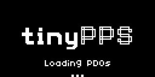
As soon as PDOs are read from the USB source or after a timeout, the number of available PDOs is printed out:

Menu screen
If more than one PDO is available, the menu screen is shown as a simple list from which the user can select the desired PDO:
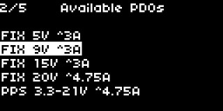
User inputs:
- rotary encoder increment/decrement: Move up/down in the menu
- rotary encoder button press: select PDO and move to main state
Main screen
This is the screen that shows the power supply user interface. It enables control and monitoring of voltage, current, and output. Besides this, it shows the active PDO type (FIX or PPS) and temperature read from the NTC in the upper corners.
The actual output voltage/current values are periodically read from INA226 and displayed with bigger font while the target/limit referent values are displayed with regular font.
On the bottom are located three boxes marked as CV (constant voltage), CC (constant current) and EN (output enable) used as status bar.
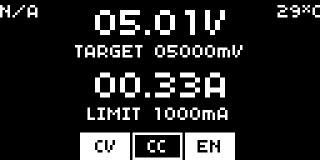
User inputs:
- rotary encoder increment/decrement:
- Select target voltage or max current fields.
- Increment/Decrement target voltage or max current values.
- rotary encoder button press: If target voltage or current limit field is selected enter value editing mode.
- rotary encoder long button press: enable/disable output.
- rotary encoder double press: Go back to menu state/screen if there are more than one PDO available.
Designing firmware to support AP33772 and AP33772S
The initial version of TinyPPS used AP33772S only. To simplify integration of the AP33772 into the main codebase, an interface (IPdSink) was created to represent a generic USB PD sink IC. It defines the necessary structures, enums, and functions required to describe such a device. This interface can also be reused in the future to support other USB PD sink ICs.
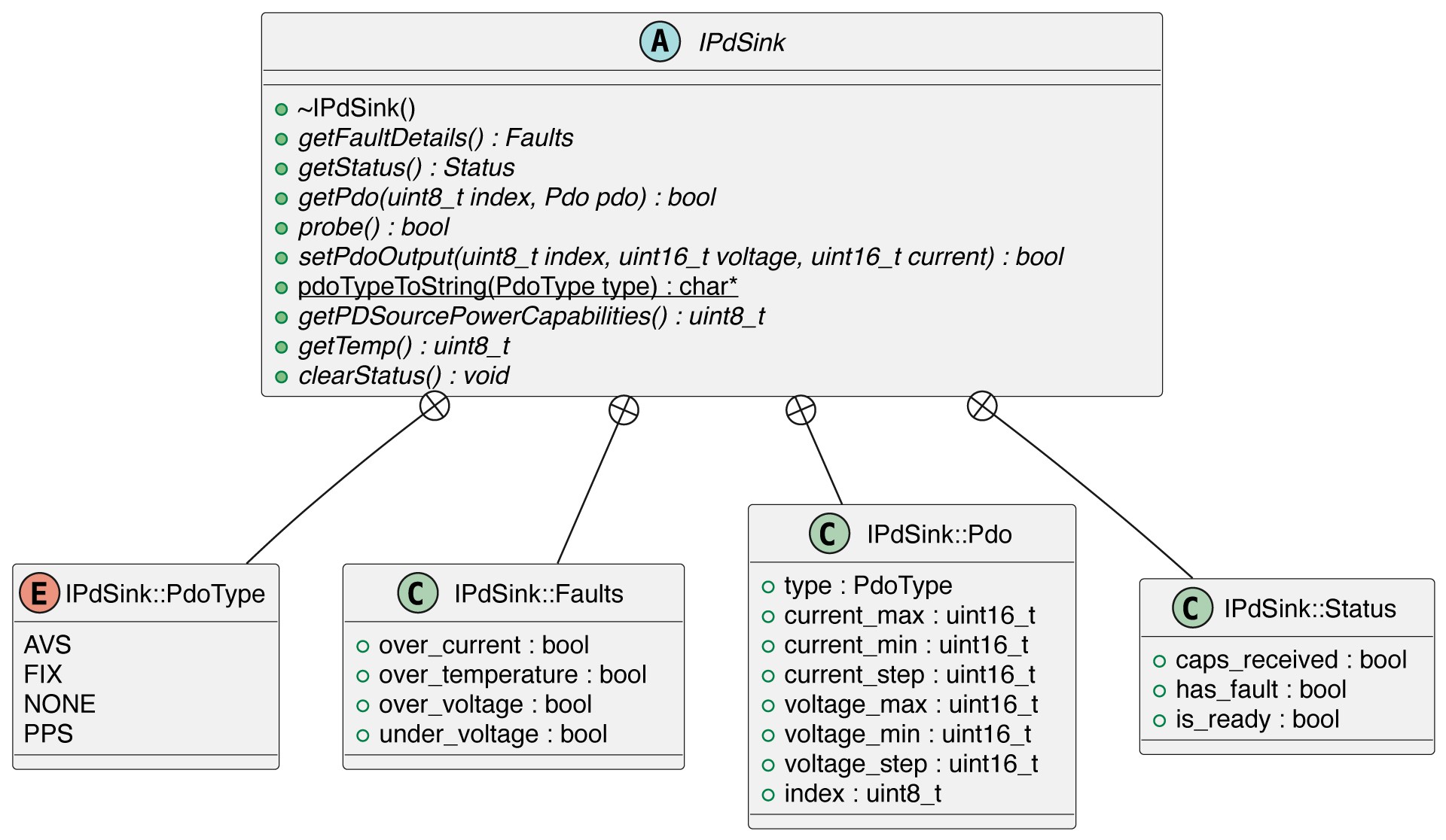
Both the AP33772 and AP33772S implement the IPDSink interface, allowing the main module to remain unaware of the specific device in use after initialization. For the AP33772S, this required only refactoring the existing implementation, while the AP33772 was implemented from scratch based on the datasheet.
The main() holds instances of both the AP33772S and AP33772 drivers. At runtime, the correct one is selected based on the detected I2C address (via the probe() function). This allows a single firmware build to support both IC variants, despite differences in feature sets. Since the two ICs are pin-compatible, this approach avoids maintaining separate firmware versions and reduces the risk of flashing the wrong firmware.
Keeping both instances pre-created simplifies the design in an embedded context:
- It avoids dynamic memory allocation
- It ensures deterministic initialization
- It eliminates the need for runtime object construction or complex lifetime management
- This approach favours predictability and simplicity over resource usage
Board bringup
Bringing a newly assembled PCB to life is always the most challenging part of a project. At this point, months of research, schematic design, PCB layout, component selection and assembly are put to the test. There are so many factors that can influence the outcome.
I started inspecting the assembled board for solder bridges and fixing them. After that, I hooked up the device to power supply and verified the 1V1, 3V3 and 5V rails using test points (I missed to add a test point for 1V1).
Next step was to flash RP2040 with a simple test firmware that toggles a GPIO pin (same as a LED blink test) to verify the RP2040 is alive. Flashing passed, but the GPIO pin remained at 0V. RP2040 was dead.
To narrow down the issue, I flashed the test firmware directly to RAM, bypassing the external flash. Surprisingly, the behavior remained unchanged. This indicated there was clearly an issue, but it might not be related to the flash.
After some time digging and using AI as a rubber duck, I found a solution. The project was configured for a predefined RP2040 board definition, which clearly did not match my custom hardware. Changing the board type in the CMake configuration to "none" resolved the issue:
set(PICO_BOARD none CACHE STRING "Board type")
With the test firmware working, it was time to flash the TinyPPS firmware onto the RP2040. As expected, it did not work on the first try. It turned out, during PCB design, I changed the I2C pins to make routing easier. But I forgot to leave a note about this change to my future self.
At the end, everything worked as expected. The happy end :)
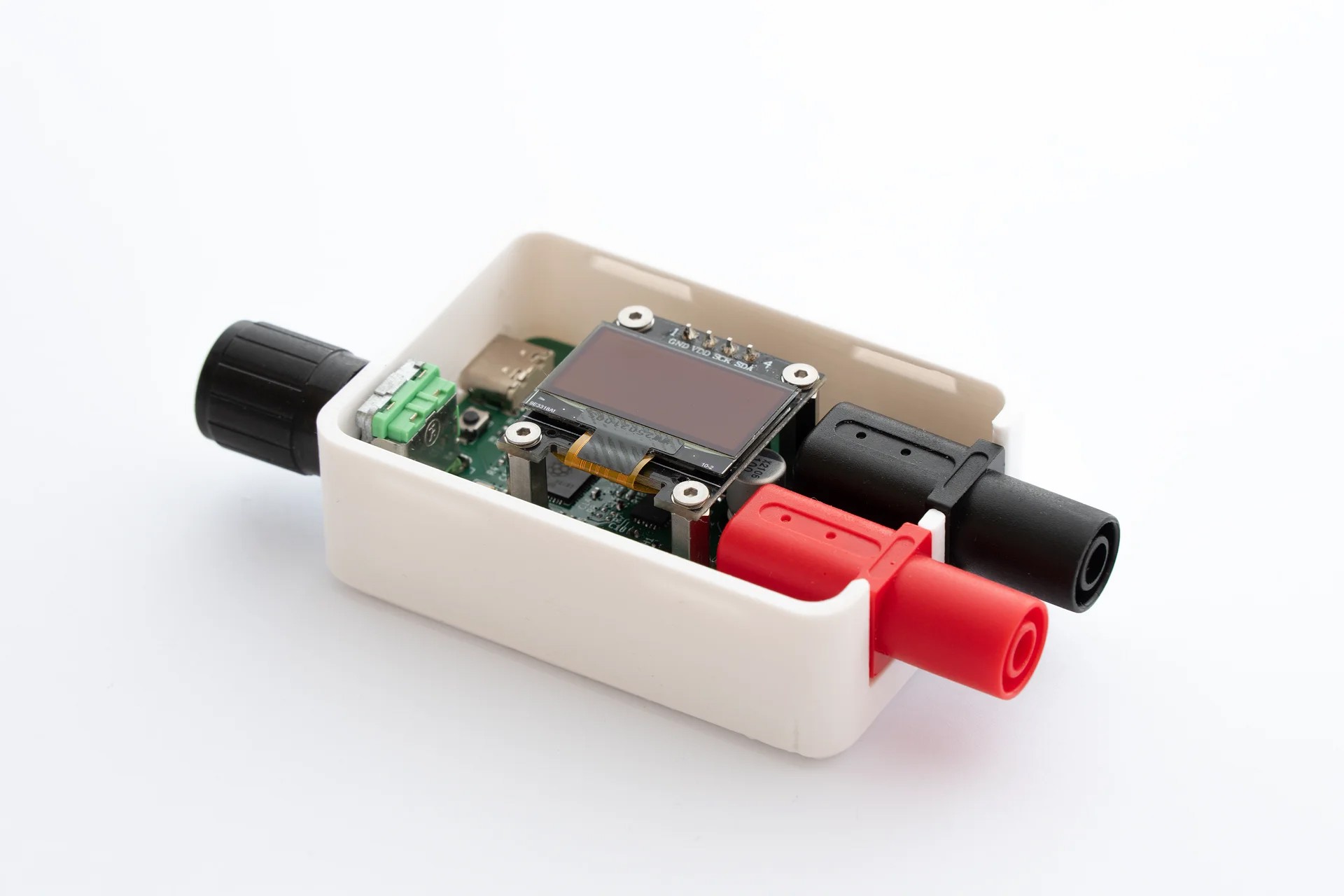
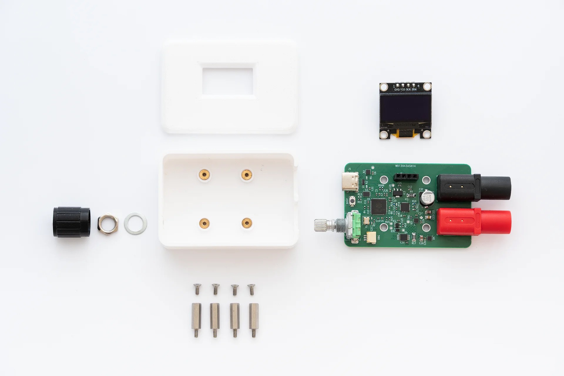
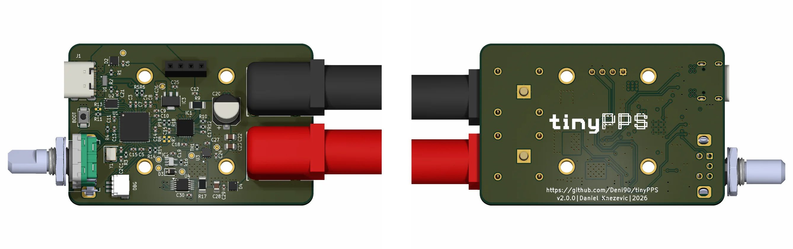
Case
For TinyPPS, I wanted to create a simple and minimalistic box-shaped case with rounded corners. The case features a snap-in lid that hides the mounting screws used to secure the OLED and PCB to the bottom part of the case.
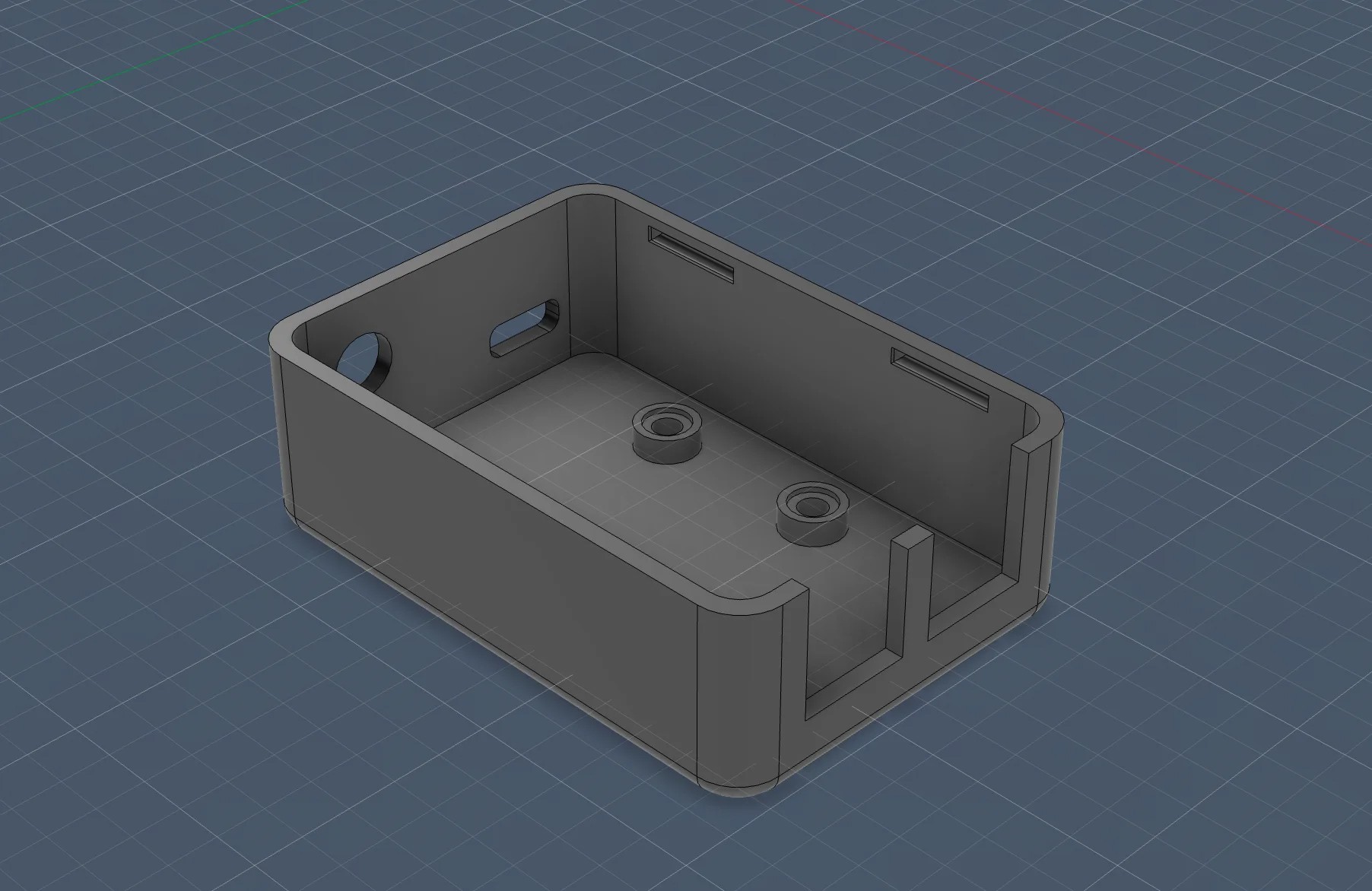
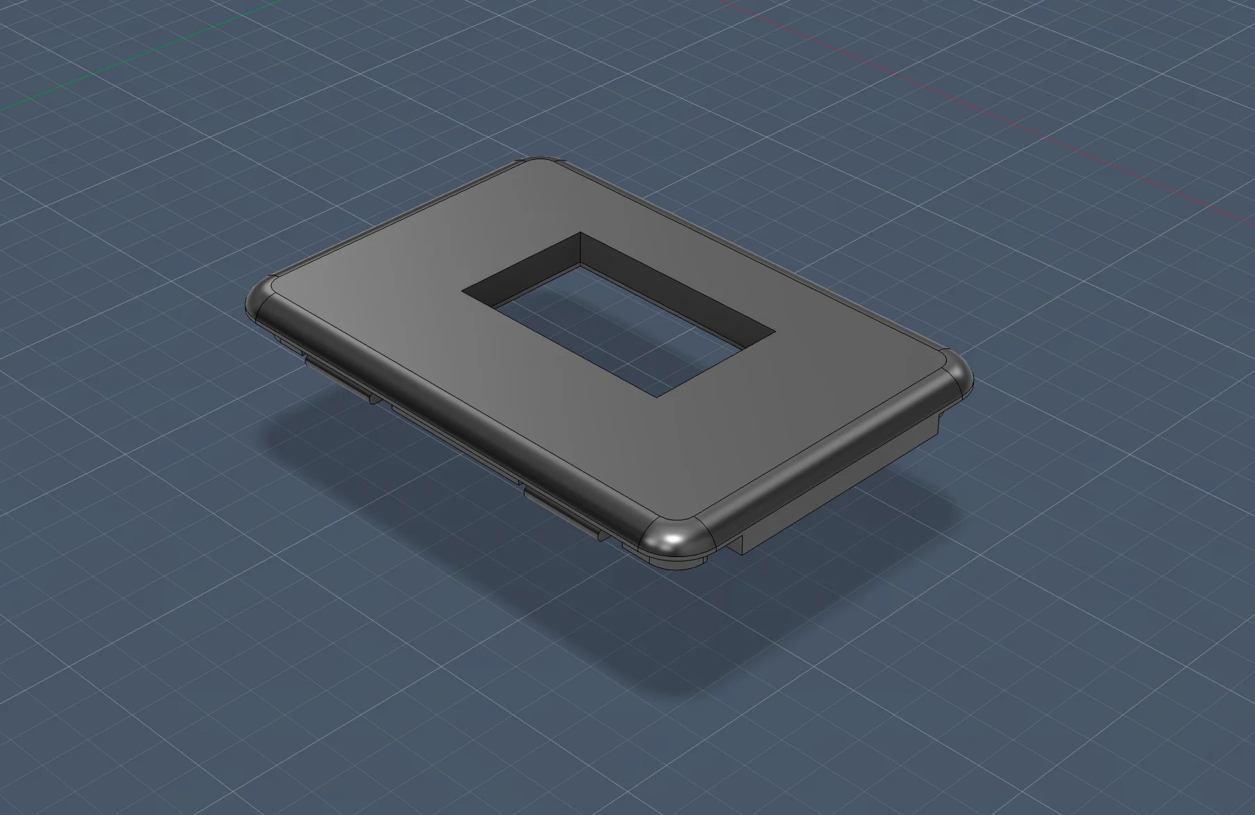
Here are some photos of the building blocks and the case: