 Marcellus Pereira
Well, the main idea was that this project wouldn’t use FPGAs. It’s not that I’m against hardware synthesis—I think it’s an incredible idea that makes many advanced projects technically and financially feasible. But I wanted to build this machine exactly as I envisioned it more than two decades ago.
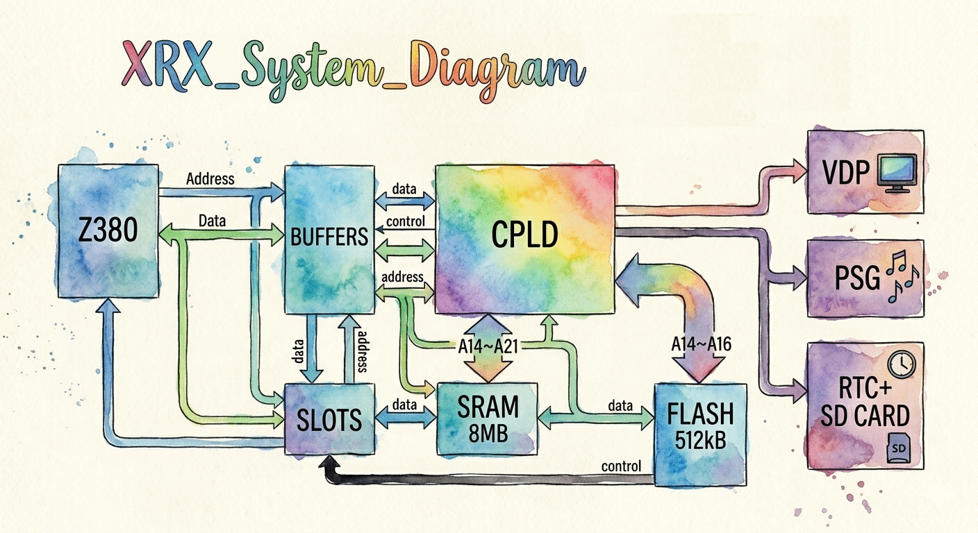
However... using dozens of logic chips these days doesn’t seem like a good idea to me either. So, I settled for a middle ground: I used a CPLD as “glue logic.” The question was: which one?
I wanted to use a CPLD that:
0. didn’t use a BGA package.
1. had enough logic elements. How many? I don’t know.
2. had 5V-tolerant pins.
3. had free development tools (they didn’t even need to be open source).
The biggest problem, in my naive optimism, was how to know if the number of logic elements would be sufficient. Knowing that the Z380 would access the VDP at four times the speed (considering only the clock, without taking the pipeline into account), I wanted to have a FIFO implemented between the VDP and the microprocessor. How many logic elements? I don’t know. Would it be possible to do this with a CPLD instead of an FPGA? I don’t know.
So, the easiest (and by far the most expensive) way was to choose the largest CPLD that met the requirements.
The choice was the Lattice LC4256V. Part of the ispMACH 4000 family, it has 256 macrocells (that number seems sufficient, doesn’t it?), is powered by 3.3V, but the pins are “5V-tolerant.” In fact, it has 128 I/O pins (that number seems sufficient, doesn’t it?). Lattice provides (provided) the development tool... so, everything seemed fine. Except it wasn’t.
To cut a long, long story short: not only was it impossible to implement the FIFO the way I wanted (though the VDP data bus is still connected directly to the CPLD), but it was also impossible to implement a memory mapper that controls more than 128kB. I know, I know... maybe it’s my lack of skill with Verilog code. But that’s how it stands for now: 8MB that the program can access linearly, or 128kB accessed via the mapper. I’ll go into more detail about the memory later.
Well then, CPLD chosen, development tool purchased... the chip in the development kit isn’t exactly the one I’m going to use, but it’s quite similar—what could go wrong? Well, the CPLD in the development kit doesn’t have “5V-tolerant” pins.
And to make matters worse, I couldn’t use the kit to program the CPLD on my board; I’d have to buy a tool from Lattice or try using an open-source project.
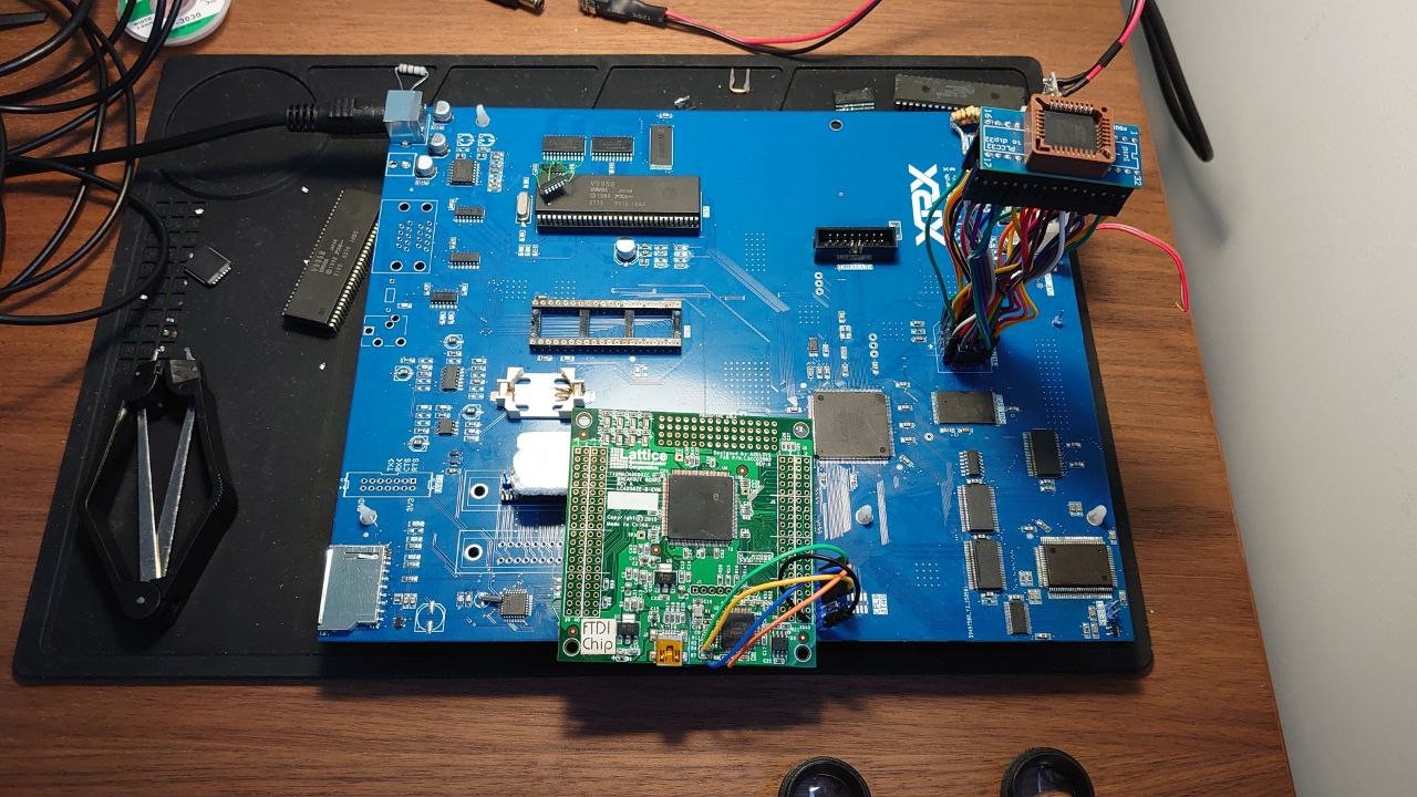
The final decision was: to create the first version of the board using the CPLD itself (instead of pin bars I could connect to the external kit) and to make a small “hack” to the Lattice development kit so I could use it as a programmer. “How hard can it be?”®
After all that, Lattice decided to stop providing free licenses to schools and hobbyists. The ispLever Classic tool now costs 600 euros... for one year! What to do?
Well, it’s time to reconnect with old friends and catch up with your old college. Maybe they still have some old computers in the digital circuits lab with a valid Lattice license. BINGO! :-)
Without getting into the legality of the solution, I could now program the CPLD on my prototype board. And considering the cost of the board *and* the components, it would be great if I hadn’t messed anything up the very first time. It doesn’t hurt to dream, does it?
Discussions
Become a Hackaday.io Member
Create an account to leave a comment. Already have an account? Log In.