 Marcellus Pereira
I spent weeks—several weeks—trying to figure out what was going on.
I wrote a very simple program that toggled a keyboard pin, and, of course, it wasn’t working. But it SHOULD have worked.
Using a data analyzer, I monitored the address bus, the data bus, and some control pins on the Flash. And it was really impressive to see just how much more advanced the Z380 was compared to the Z80. Of course, you already know this from reading the manual, even though the manual is pretty superficial. But it’s one thing to read about it and another to *experience* it.
Instructions executing in just a few clock cycles, the I/O bus completely separate from the memory bus, the internal (“phantom”) registers that simulate an instruction fetch cycle… it was an invigorating experience. So much so that I asked the chip’s architect for an autograph (more on that later).
During that time, I discovered two things. The first is that I had completely messed up the pinout of the Flash memory socket.
The second is that I had routed the SRAM data pins incorrectly.
<<Insert happy face here>>
This took me some time because the ROM is accessed in bytes; so to read a 16-bit value, the Z380 uses two fetch cycles. RAM, on the other hand, is accessed in 16-bit words, meaning that to read the same value, the Z380 uses only one fetch cycle.
Since the ROM can be accessed in both slot 0 and slot 3, I spent my time looking for issues in the Verilog code for the slot selector, instead of focusing on the hardware.
By the way, here is the slot map:
```
+------------------+--------+----------+----------+--------+--------+--------+--------+
|                  | Slot 0 |  Slot 1  |  Slot 2  |Slot 3-0|Slot 3-1|Slot 3-2|Slot 3-3|
+------------------+--------+----------+----------+--------+--------+--------+--------+
|  10000h~7FFFFFh  |        |          |          |  8MB   |        |        |        |
+------------------+--------+----------+----------+--------+--------+--------+--------+
| Page C000h~FFFFh |        |          |          |        |        |        |        |
+------------------+        |          |          | 128kB  +--------+        |        |
| Page 8000h~BFFFh |        |Cartridge |Cartridge | Memory |        |        |        |
+------------------+--------|  Slot 1  |  Slot 2  | Mapper | Kanji  |        |        |
| Page 4000h~7FFFh |        |          |          |        |        |        |        |
+------------------+  Main  |          |          |        +--------+        |        |
| Page 0000h~3FFFh |  ROM   |          |          |        |Sub-ROM |        |        |
+------------------+--------+----------+----------+--------+--------+--------+--------+
```
Since there was no use crying over spilled milk, I rolled up my sleeves and went back to the drawing board. I mean, to the CAD.
I redesigned the board (still without the “X-Slot”), taking the opportunity to fix a few other minor slip-ups. One of them I later regretted: I had planned to include a UART, which would be implemented by the same microcontroller that would simulate the RTC. If I had kept that “feature,” my debugging sessions with the new board would have been much easier.
Anyway, I also decided to have the board assembled by the supplier (I won’t mention the name here because they aren’t sponsoring me… but you know who I mean). For the first two versions, I soldered the components myself. But let’s face it, I’m past that age. I don’t have a microscope here, and soldering components with a 0.4mm pitch… so I took the easy way out.
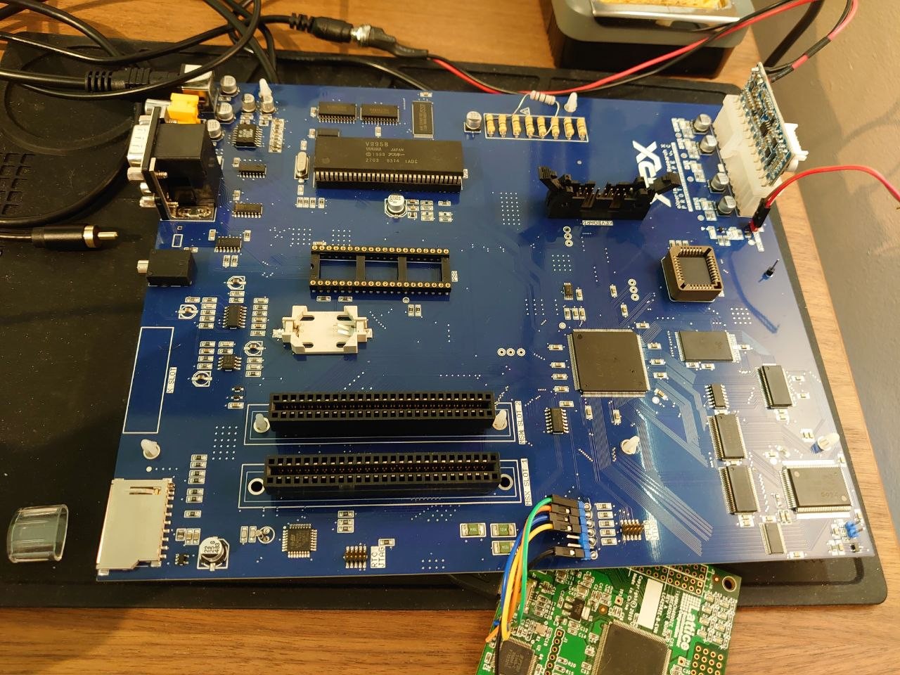
That saved me A LOT of time. Instead of spending days looking for a defect that wasn’t in the Verilog code or the assembly code, but rather a smudge of solder under a CPLD pin, I was now pretty sure the hardware was right. Or rather, I was sure that the board I had in my hands was exactly the one in my CAD.
But I was now facing two problems. While the hardware was reliable, there were still the Verilog code and the assembly code to consider. Despite the verification and simulation, the CPLD was programmed to do what I *thought* it should do, with several “shortcuts” to save a few logic gates. And since the first attempt to run a “real” MSX BIOS hadn’t worked, it was obvious that there were still some problems to solve.
The solution, as Jack the Ripper would say, was to take it step by step.
Creating an MSX machine for OpenMSX would help me a lot. I could create a more advanced test program and be sure it would work on an MSX “machine.” After finishing the program, then I would flash it and test it on real hardware.
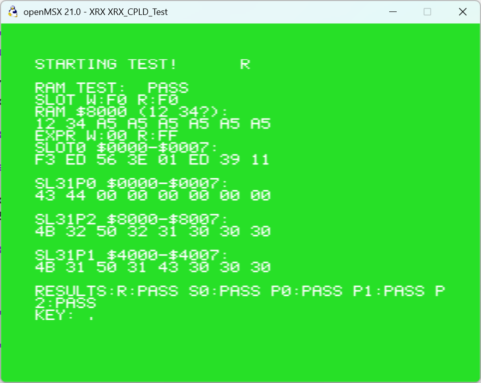
And so it was done. I created a small program that tests the memory mapped in slot 3-0, the sub-ROM on page 0 of slot 3-1, and the kanji driver on pages 1 and 2 of slot 3-1. This would validate my entire Verilog implementation of the primary slot selector, the slot expander, and the memory mapper.
If everything went well, this should be the result on the actual hardware:
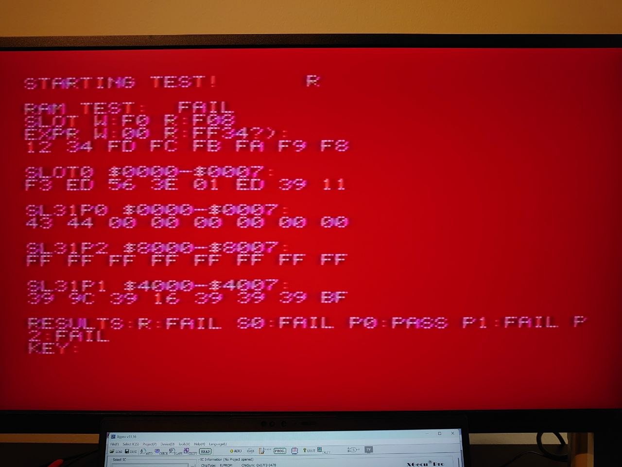
The time had come. Without giving it much thought, I reprogrammed the Flash (the *only* one I still have, since I broke a terminal on the other one), took a deep breath, and turned on the power supply. Nothing.
Oh! I also had to change the monitor’s video input… and then:
Sometimes—just sometimes—I find the MSX “slot” system a bit confusing. Slots. Sub-slots. Memory mapper. Pages. Mushrooms. Oh, wait, that’s a different Japanese system.
Well, after some work on the Verilog code, lo and behold:
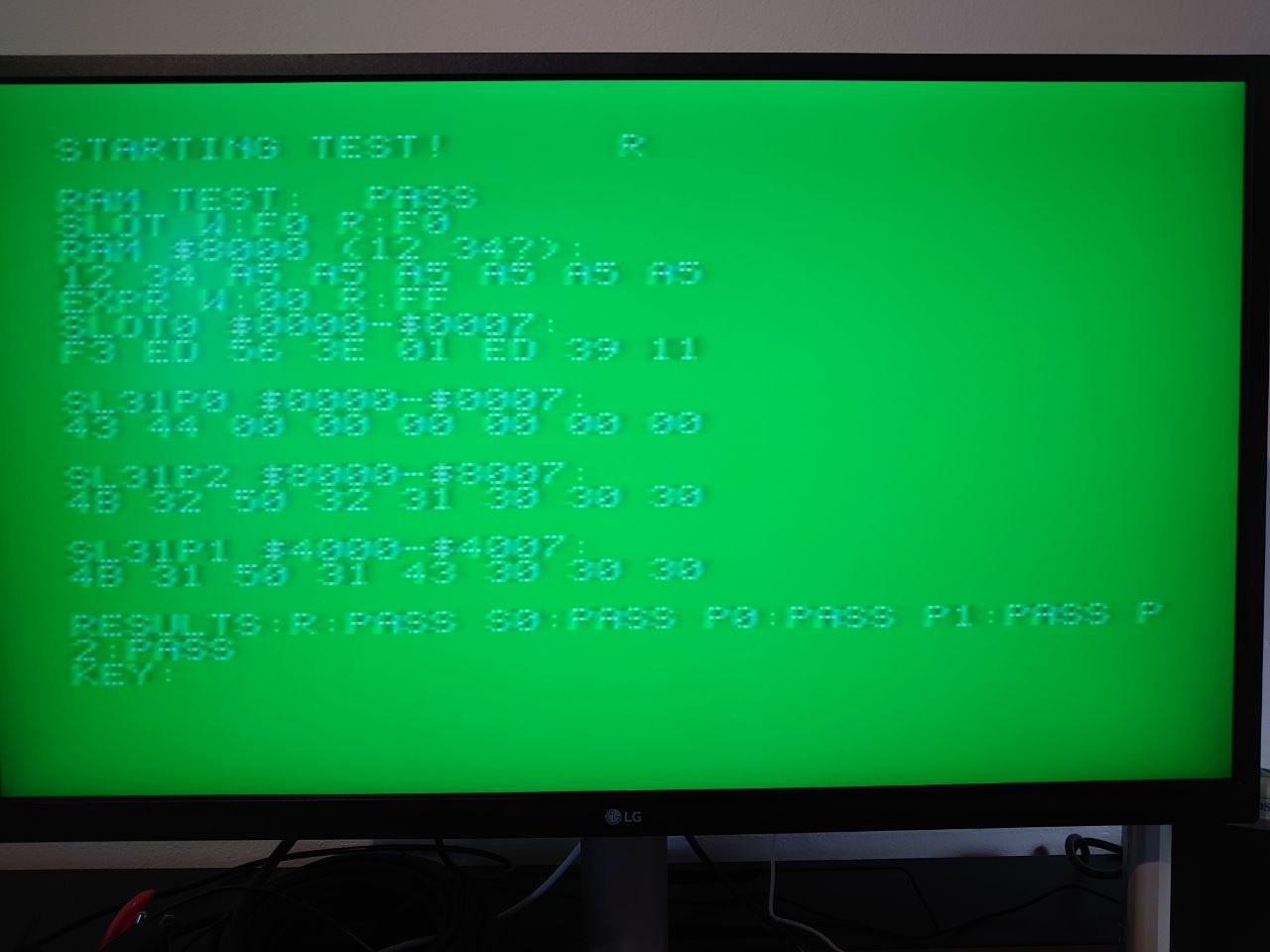
A happy face at last.
Discussions
Become a Hackaday.io Member
Create an account to leave a comment. Already have an account? Log In.