 Marcellus Pereira
Last time, the walls came down. This time, we understood why. All five walls of them.
Yes. Five. But let’s not get ahead of ourselves.
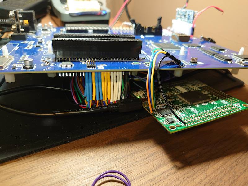
With the CPLD test program running smoothly, I was feeling pretty confident. The slot selector worked, the sub-slots worked, the memory mapper worked. Almost too good to be true. <<Insert a happy smile here>>
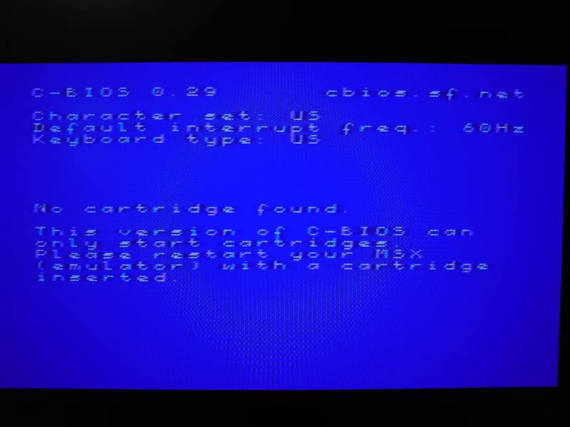
Instead of using an MSX2+ ROM, which would be very difficult to modify, I chose to use C-BIOS, a community project for a basic BIOS for MSX computers that avoids proprietary solutions and was designed for use in emulators. It’s not exactly what we need, but the available source code is a huge help.
After a quick modification, it was being compiled by ZDS—Zilog Developer Studio—for the Z380. I didn’t make any major changes, just the initialization of the internal registers.
I burned the BIOS and the sub-ROM to Flash memory and… garbage.
And not even the kind of garbage that’s one person’s treasure. Random garbage, different with every boot.
Wall Number One: The Ghost Slots
C-BIOS searches for RAM by writing a byte and reading it back. Makes sense, right? Except that, on this board, an *empty* slot responded to the command. The data bus, apparently due to parasitic capacitance, retains the last value written to it—so the C-BIOS wrote a byte into the void, the void politely echoed it back, and the C-BIOS happily selected a slot with no memory chip. My machine believed in ghosts.
The fix was made in the CPLD: any read of a slot that doesn’t have an actual device behind it now returns $FF. No more séances on my data bus. It’s not the definitive solution, but it’s what we have for now.
Wall Number Two: The Lying Registers
It was possible to write to the slot registers, but when I read them, they returned a strange value. The CPLD was recording the read data at the bus clock—one cycle late, every time. A flip-flop was downgraded to a transparent latch, and the registers stopped lying.
Wall Number Three: The Two Worlds
This was the big challenge—the one that had been haunting this project for *months*.
The code copied into RAM refused to run. It wasn’t a “spectacular failure”—it was worse. It would run, return, and politely spit out garbage. Always the *same* garbage.
I had to connect almost all the cables on my data analyzer. It looked great on the board; I had to solder a few terminals on the underside… but the data analyzer finally revealed what was going on. The Z380 writes individual bytes using address parity: even bytes here, odd bytes there. But when it *fetches words*—and fetching instructions from RAM is always done in words—it uses aligned addresses. My SRAM had its A0 pin connected directly to the CPU’s A0 pin, so that bytes written one way couldn’t be found the other way. Two parallel worlds—the world of bytes and the world of words—sharing a single chip and never agreeing on where things were. And here I was, thinking I’d eliminated all the bugs from the schematic.
Every byte the program wrote to an odd-numbered address simply *didn’t exist* for the instruction fetcher. The C-BIOS copies its slot-switching routine to RAM and jumps to it. You can imagine how that turned out.
The solution? A wire. I lifted pin A0 on the SRAM (remember: 0.50mm pitch, no microscope), soldered it to ground, and let the byte enable signals do their job. In Brazil, we call this a *gambiarra*, and I’m not ashamed of it. Well, maybe a little, but it’s a temporary fix.

Wall number four: the impatient CPU
With the RAM finally coherent, the C-BIOS booted up… and generated garbage again. But now it was *stable* garbage. *Good* garbage. Not a treasure, but good garbage.
Progress!
The V9958’s datasheet is quite clear: a minimum interval of 8 µs between VRAM accesses. The Z380, with its pipeline and four-IOCLK I/O transactions, hammers the poor VDP every 2.2 µs (if the clock is 3.58 MHz—imagine when I enable the 14 MHz!), at least when the C-BIOS uses the "otir" or the "inir" instructions. Reads would come back duplicated—the VDP’s read buffer was read twice before it was modified—and writes would simply disappear.
So, the BIOS learned some manners: every access to the VDP on this machine is now followed by a short delay loop. The VDP gets its 8 microseconds. Everyone’s happy. I’m still figuring out how to solve this in the CPLD.
Wall Number Five: The Interrupt That Interrupts The Interruption
We’re almost there. The screen worked… once every few boots.
The culprit: the VDP interrupt firing in the middle of a VRAM operation, and the interrupt handler reading the VDP status register while the poor chip was in the middle of an operation. The completion of the initialization routine depended on where the vertical blanking interval happened to fall. Maybe it’s because the C-BIOS was designed solely for emulators, maybe on emulators the initialization is faster than on actual hardware, or maybe I’m completely off base here.
The fix has two steps: during boot, the VDP interrupt is simply not enabled until the entire boot process is complete. And at runtime, every VDP operation is now atomic—interrupts wait their turn in the queue. It’s not the ideal solution either, but I wanted something running, even if it’s a little slower than it could be.
Temba, his arms wide
I flashed everything once again. C-BIOS banner. Reboot: C-BIOS banner. Power cycle: C-BIOS banner. Reboot: C-BIOS banner. I kept going well past the point of statistical significance, smiling the whole time. Smiles have been few and far between on this project.
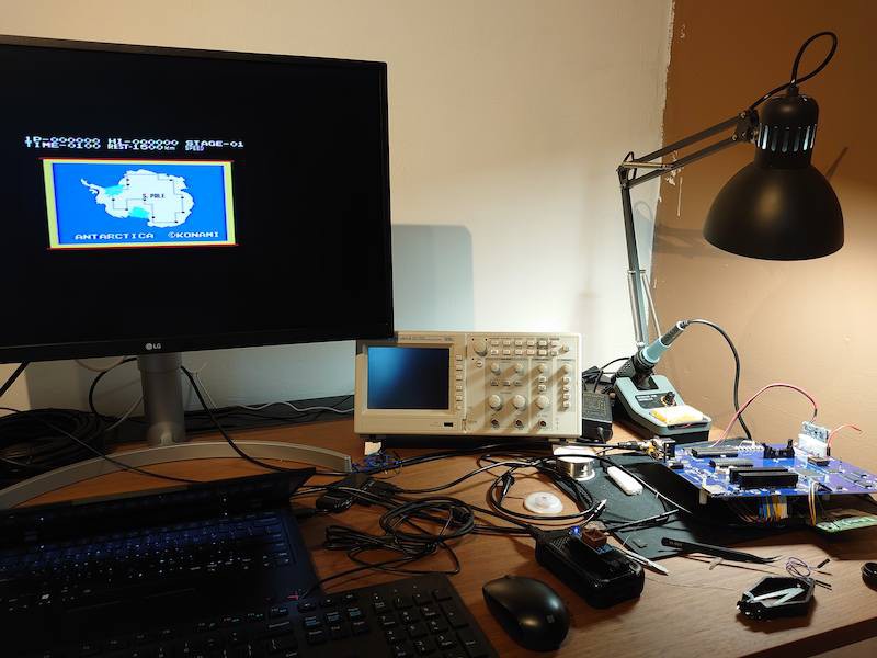
So, since a stable C-BIOS banner is cool, but no one frames it and hangs it on the wall, I burned a 16kB ROM to the flash memory—exactly where slot 3-1 maps to page 1—and turned on the computer.
A penguin. Gliding across Antarctica. On a Z380 that, years ago, was just a spec sheet and a terrible idea.
There’s still no audio—that’s for later.
By the way, you know that story about the chip architect’s autograph? Yeah, we haven’t talked about that yet. We’ll talk about it. But not today. Today is a day to celebrate.
Discussions
Become a Hackaday.io Member
Create an account to leave a comment. Already have an account? Log In.