 Parallel Logic
One of the very first risk-reduction activities I did was to inspect how difficult it is to run Python on the Pico2 (RP2350A with 4MB Flash), running across the dual cores. Findings:
- Core0 executes MicroPython out of Flash, which means core1 doesn't have Flash access. Any data that core1 operates on needs to comes from shared memory between core0 and core1 (there is also a FIFO that raises IRQ events, but that's more for flagging transfers than to actually bulk-transfer data)
- I'm not entirely clear how much of a performance hit running Python on a core is vs running C. I opted for C++ code on Core1, accessible as a library in Python in core0. This allowed me to prototype the C code portion standalone in the Arduino IDE (this is the contents of the src/experimentation/ folder)
- The original vision was to have core0 perform administrative functions "draw a rectangle here" and core1 would perform them "pixels x-y in this list are now this value, 'for' loop runs...". Core1 would also handle all the peripherals.
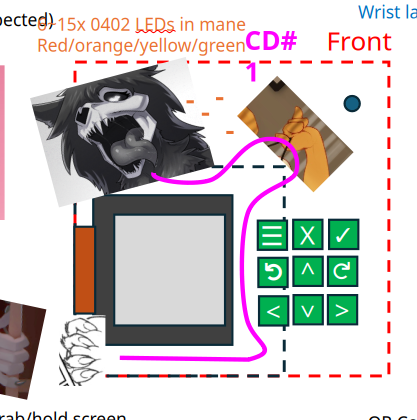
First concept layout
- I had early notions of a leash of LEDs going from her neck all the way around the screen. Later, when I laid this out to scale, the cap touch buttons needed to be so large, there wasn't good clearance between the touch pads on the right and the screen on the left (plus I has EMI/EMC concerns between the sensitive cap touch pads and the high frequency charlieplexed LEDs), so I ultimately broke this string of LEDs into two banks: one in her hair, and one as a kind of status/scroll bar below the screen - giving the cap touch pads a clan shot directly into the processor (where I'm trying to measure capacitance changes on the order of 10s of pF).
- I opted for red-green LEDs, on the premise the primary color of SCP content is a shade of orange (mix of green and red). Chareliplexing N pins allows control of N*(N-1) LEDs - ex for 8 pins that's 56 LED elements. The width of the screen fit around 24 LEDs (24 red-green LEDs is 48 LED elements). So I moved forward with a lower bank of 24 red-green LEDs below the screen, and an upper bank of also 24 LEDs. This allowed me to recycle the same PIO/code interface between the LED banks.
- I considered WS2812 LEDs to get full RGB support (also called "NeoPixel"s by Adafruit). The SAO standard stipulates 3.3V input, and I disliked the idea of needing to add a 5V step-up converter required by the WS2812s. I wanted to keep the BOM cost reasonable, so opted for dumb LEDs (with a 1.8~2.3V forward voltage) with a plan to Charlieplex them (requires floating most of the GPIO pins in a bank, and then driving one pin high, one pin low, holding that for a tiny fraction of a second, then moving on to the next pairing). The RP2350 supports floating the pins through PIO, where the prior generation chip did not. The impact of chareliplexing LEDs vs a serial string of WS2812 is that it notably complicates PCB layout since there is now a direct electrical connection from LED directly to the processor (vs just a chain connection to each LED's neighbor in WS2812).
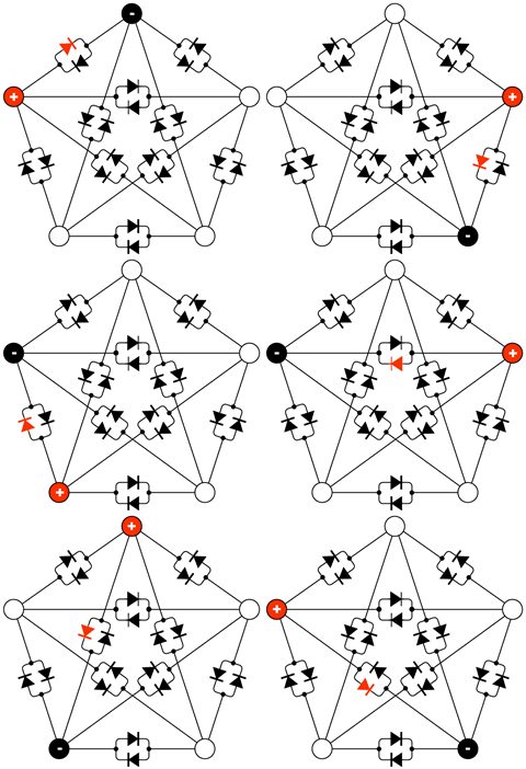
- Those reviewing this closely will note the processor runs at nominally 3.3V (per the SAO standard), but the green LEDs wants ~2.9V and the red ~2.1V. There is a dirty trick where high current draw (~20mA) through the processor will actually drop the drive voltage a bit, so I actually drive the green LEDs straight off the RP2350 GPIO pins. For the red, I did include a resistor dropper, but I kept it to only 3 resistors total across the entire bank of 8 GPIO pins. I did this by carefully selecting grouping of red LEDs to all share a common pin and routed the red connections through the resistor before reaching that gpio pin.
- All this work was done before the DEFCON34 MICD was released. At this stage, I was very concerned about overall size and keep-out zones. Most SAOs gravitate to around 2~2.5" max outer dimensions, but this quickly expanded past 3". I also assumed that the major keep-out zone would be below the SAO, so I worked to keep the PCB real estate south of the SAO as limited as possible
- I wanted to keep the design elegant, and my definition of that is as few holes showing through the board as possible (really want to highlight the final artwork as much as possible). I opted for a USB-C port where I could hide the structural holes behind the screen. I also had a surface mount SAO header on this prototype.
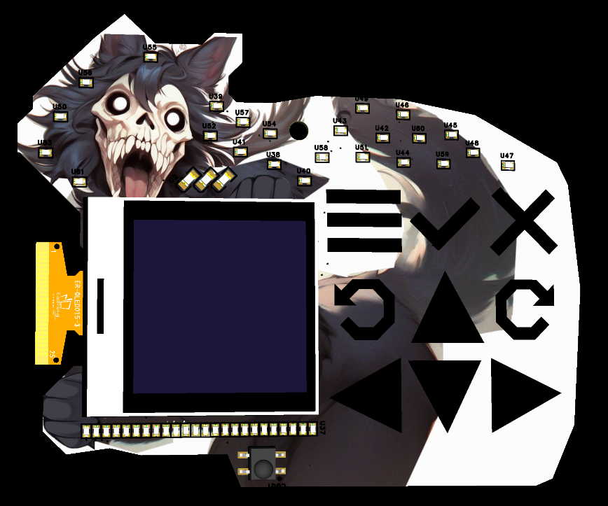
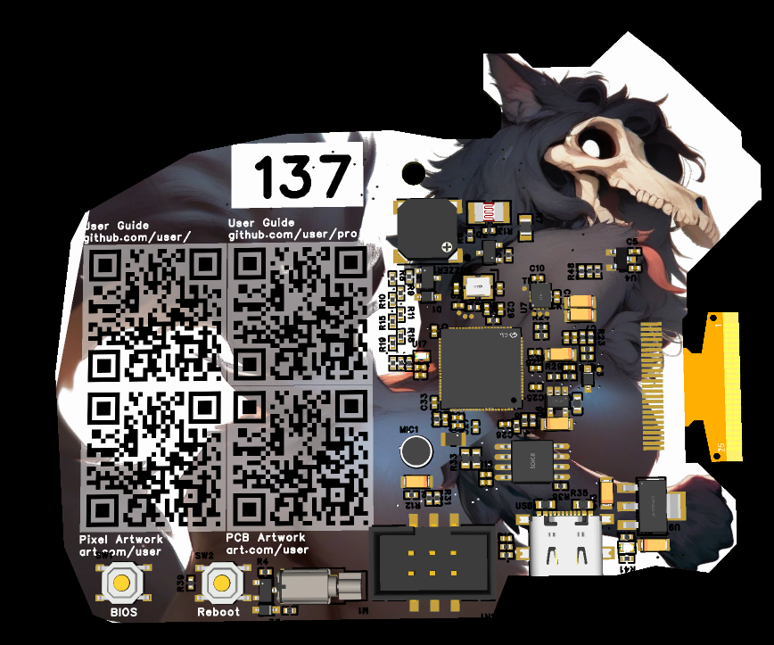
- I've been told it's wise to give each PCB a serial number. JLCPCB now does this automatically for you if you want, but only for standard silkscreen (cannot be selected for RGB silkscreen I'm using here). So the fall-back option is a big white square where the serial numebr can be hand-written in.
- The area behind the cap touch keys needs to be devoid of parts to avoid coupling interfering with the measurements. This naturally paired with QR codes. I had a notion of a link to the Github user guide, and to the two artists I'm working with (one for PCB/sticker artwork, one for pixel artwork). However, per some user feedback, later revisions simplified this to a single gihub.io splash page that has several links off from there.
- There's an inherent chicken-and-egg dynamic between the layout and PCB artwork. To try to decouple that, I opted to just use a generic AI generation on this first prototype.
- Cap touch to me seemed the biggest risk, so I actually tried two different routings on this first prototype: the main set of 9 buttons have a 1 MOhm resistor to ground. To take a measurement, the PIO pin is tied to 3.3V, then floated, then the pins are read/polled until they schmitt trigger below the cut-off voltage to read as a '0'. This is a hacky way of measuring the decay constant of an RC circuit. It should also be noted this only works on the A3/A4 stepping of the RP2350. If you have a Pico2 with "A2" at the end of the chip name on the board, then erratta E9 applies where there is a relatively huge current leak on the GPIO pins, making cap touch (and anything less than ~8 kOhm pull up/down) not work on those models of chips.
- The super secret super snooper booper button (spoilers) I routed differently, replacing the ground connection with a PWM pin. In this way, I can set the PWM to toggle at a constant rate and leave the cap touch pins as constant high-impedance inputs (just polling for 1/0 state changes) - just looking at how long it takes for them to change state relative to the PWM pin. This saves me from having to toggle between modes with the PIO assembly instructions.
- Eccentric vibrating mass aka vibration motor I setup so it's pointed at the SAO header on the hopes that if it's shielded on two sides (motor housing and SAO header) it's a little less likely to get caught up in fabric the user is wearing.
- The photo-resistor was a late removal. I show it here on the prototype as I submitted it, but the fab house flagged it as something they'd have to drop their reflow temperatures to comply with (ie. the part is designed for leaded reflow temperatures, but China generally uses unleaded, which is ~30 C hotter). Rather than paying a bunch extra to process the board as I originally designed it, I swapped it out for an I2C photosensor for the final submission.
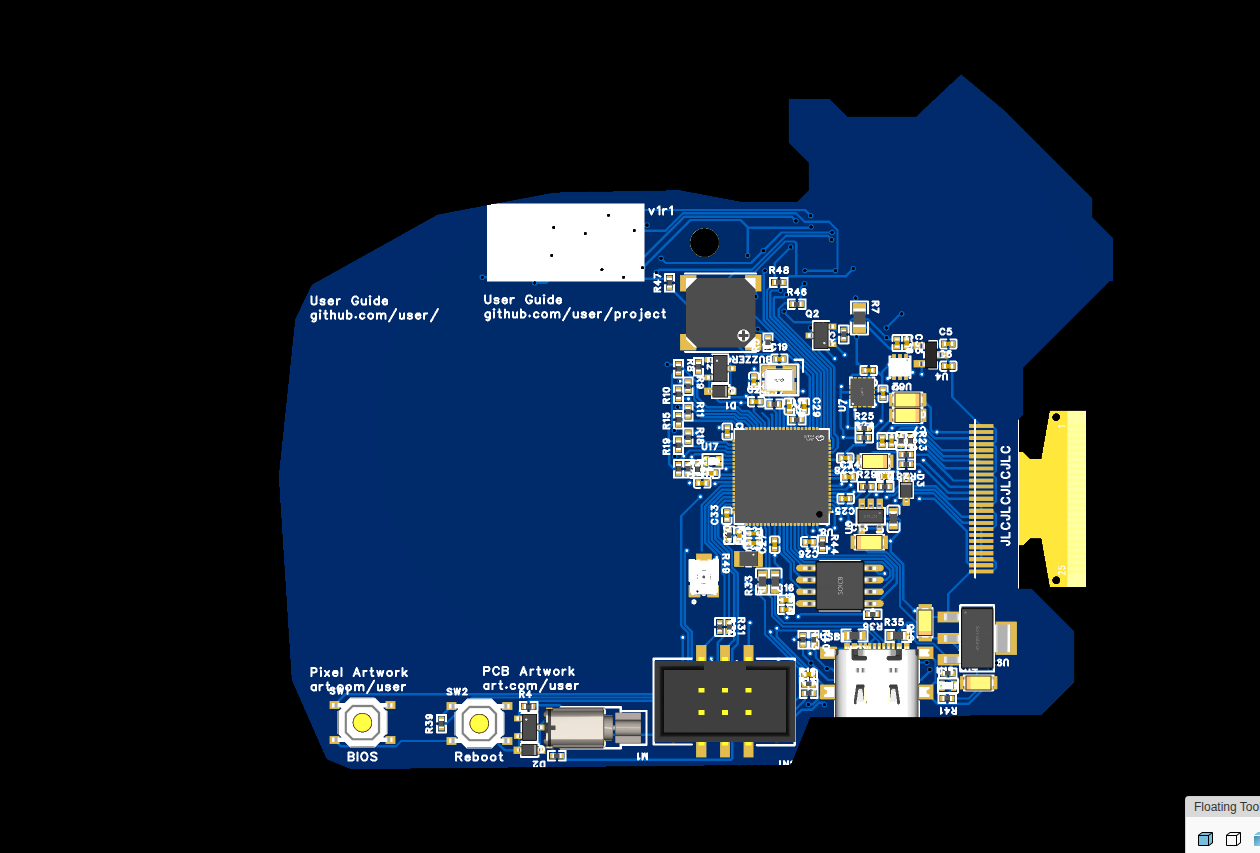
- Layout itself went relatively smoothly (I'm quite fond of how the chareliplexed LED lines all go up in parallel together North of the processor). The rat's nest had something like 300+ connections that it took me a week or two (working in the evenings and weekends) to connect. The real trick is planning out which parts will go to each GPIO pin so they can be organized radially in that order. There's something about the RP2350 I'd call "academic" where the design decisions seems very clean and symmetric. Most processors will have 4~8 functions each pin can perform and there's a calculus to figure out which ones can be assigned to which peripheral. The RP2350 seems more relaxed in that regard where virtually everything can go to almost any pin (to the point I had some analysis paralysis where many peripherals could go to many pins). There are some constraints, like all the analog pins have to be next to the USB since that's the only ones plumbed for analog input. Any pins being driven by PIO should all be grouped in a uniformly-increasing sequence together since that's how the PIO expects to update them. There are only two SPI and two I2C hard IPs (yes, the PIOs can mimic that to an extent, but it's extra complexity) - so it's important to track which sensors are on the i2c0 line vs the SAO i2c1 line. A late find is that if you want to drive PWM on pins, you'll want to track which bank each pin is on - neighboring pins are often on the same PWM port and must be driven at the same frequency (useful for H-bridge control on motors but not applicable here).
- Every PCB layout seems to have a bottleneck of some kind - something where you can show a closed form solution that stacking up all the design rules means that two parts can only be so close, or there can only be so many electrical connections between point A and B before you max out the width of the circuit board. In this case, the LEDs below the OLED were the tightest part of the design, requiring multiple passes and tweaks ebfore I got them all to fit.
Questions/comments/thoughts/requests encouraged
Discussions
Become a Hackaday.io Member
Create an account to leave a comment. Already have an account? Log In.