 thomaswust79
It turns out that "future" arrived faster than expected. A new gateware/ subdirectory has landed in the smiSDR repository, and it is not a proof-of-concept sketch — it is a fully-verified, Verilator-simulated, multi-vendor-portable Verilog core that does exactly what the roadmap promised. This article is a technical dive into that gateware: the in-band signaling scheme that lets control and data share a single bus, and the DUC pipeline that turns a 250 ksps–1.25 Msps baseband stream into a spectrally clean 50 Msps RF signal.
1. Why Offload Mixing to an FPGA at All?
In the original architecture, any frequency translation (shifting a baseband signal up to an RF carrier) had to happen in software on the host PC before the samples ever hit the network. That works, but it wastes the one resource that made osmo-fl2k-style transmitters attractive in the first place: cheap, high-bandwidth raw sample throughput. Streaming already-upconverted RF samples at, say, 50 Msps over Ethernet or PARLIO consumes far more bus and network bandwidth than streaming baseband I/Q at a few hundred ksps and letting the hardware do the up-conversion locally.
The gateware README frames the motivation succinctly: move the Numerically Controlled Oscillator (NCO), the mixer, and the rate conversion into the FPGA, and you get three things at once:
- Bandwidth relief on the smiBus/PARLIO link — only compact baseband I/Q needs to cross the wire.
- Hardware-native DUC for TX and DDC for RX — the same generalized core is designed to run in both directions, which is the structural prerequisite for turning this into a full transceiver rather than a transmit-only toy.
- A wider usable RF span, since the mixer is no longer limited by host CPU cycles but by DAC sample rate and FPGA clock budget.
The published block diagram is refreshingly symmetric: a host system feeds baseband I/Q across the smiBus into a "Generalized Verilog FPGA Core," which contains an I/Q interface, a shared hardware NCO, a DUC path toward an external DAC, and a DDC path from an external ADC back to the host. Only the DUC half is implemented and hardware-verified today — but the DDC entry points are already drawn into the architecture, not bolted on as an afterthought.
Target Silicon
The core was explicitly written to avoid vendor lock-in and to stay within the reach of hobbyist budgets. Three FPGA families have already been used for testing:
| Vendor | Confirmed Families | Notes |
|---|---|---|
| Intel/Altera | Cyclone IV, Cyclone 10, MAX 1000 | Classic low-cost families; MAX 1000 is a particularly compact dev board |
| Lattice | "Various mid-class boards" | Popular with fully open-source toolchains |
| Gowin | Sipeed Tang Nano / Tang Primer series | Extremely cheap ($10–$30), good OSS toolchain support |
This spread matters editorially: it means a maker isn't locked into a single, possibly discontinued board to reproduce the project — a lesson the community learned the hard way with the FL2000 chipset.
2. Sharing One Bus for Data and Control: The In-Band Signaling Protocol
Both the SMI bus on the Raspberry Pi and the PARLIO peripheral on the ESP32-P4 expose a 16-bit-wide parallel word, clocked by a continuous CLOCK line and qualified by a VALID_DATA/write-enable strobe. The DAC/ADC front-ends the project targets (referred to as "Steamlab"-class parts in the documentation) are natively 14-bit devices, which leaves exactly two spare bits per word — and the designers used them cleverly instead of adding a second control bus (I²C/SPI) that would have needed extra wiring and synchronization logic.
2.1 The 16-Bit Word Map
Bits [15:14] act as a two-bit packet-type tag that the receiver decodes on every single clock:
| Word Type | Bit 15 | Bit 14 | Bits [13:8] | Bits [7:0] |
|---|---|---|---|---|
| I-Sample | 0 | 0 | — | 14-bit I data |
| Q-Sample | 0 | 1 | — | 14-bit Q data |
| Command Init | 1 | 0 | 111111 (sync) | 8-bit ASCII command |
| Param Chunk | 1 | 0 | 6-bit counter (0, 1, …) | 8-bit parameter byte |
| Command End | 1 | 1 | ignored | ASCII 'E' |
Streaming I/Q data therefore costs nothing extra — the two tag bits ride along with every sample, and the absence of a command sequence is simply the default "streaming" state. When the host wants to retune the hardware NCO or change the interpolation rate, it interrupts the stream with a short, self-delimiting command burst:
[0][0][ I-Data 14-bit ] ← normal streaming
[0][1][ Q-Data 14-bit ] ← normal streaming
[1][0][ Index: 63 ][ 'S' ] ← Command Init: begin frequency-shift command
[1][0][ Index: 00 ][ byte 0 ] ← Param Chunk: LSB of the new FTW
[1][0][ Index: 01 ][ byte 1 ] ← Param Chunk: next byte
[1][1][ Index: 00 ][ 'E' ] ← Command End: latch and execute
[0][0][ I-Data 14-bit ] ← streaming resumes
[0][1][ Q-Data 14-bit ]
Two currently-defined command opcodes exist at the protocol level — R (sample-rate selection) and S (frequency-shift/FTW programming) — plus the mandatory E terminator. The scheme is explicitly documented as backward compatible with the existing smi_tcp_streaming_dac.c host driver, so no software rewrite is required to keep older transmit-only setups running unchanged.
2.2 Two Design Details Worth Noting
A protocol like this lives or dies on edge-case robustness, and the implementation notes show the authors thought about exactly that:
- I/Q phase alignment. Because I and Q samples necessarily arrive one clock apart on a shared bus, the receiving gateware latches the I-sample into a holding register and only pushes the pair into the DSP pipeline once the matching Q-sample (tag
01) arrives — guaranteeing both halves of a complex sample enter the mixer on the same clock edge, with no phase skew between them. - Self-healing parameter assembly. The 6-bit running counter in bits
[13:8]of each Param Chunk means the state machine can detect a dropped or reordered byte instead of silently corrupting a 16/32/64-bit register, and the reserved index value111111doubles as a hard reset for the whole command parser — a cheap but effective safety net against a wedged host application.
3. Inside the DUC Pipeline: From 1.25 Msps Baseband to 50 Msps RF
The real substance of this release is the gateware/DUC/ folder: a fully-pipelined, strobe-synchronous upconverter chain that takes baseband I/Q at 250 ksps, 500 ksps, or 1.25 Msps and produces a uniform 50 Msps output stream ready for a high-speed RF DAC. The whole design deliberately avoids multi-clock-domain crossings — everything downstream of the host interface runs from strobes derived from a single core clock, which sidesteps an entire category of CDC metastability bugs that plague less careful multirate designs.
3.1 Full Signal Chain
Host DMA (SMI/PARLIO Bus)
│ 16-bit async data + strobe
▼
smi_rx_16bit → In-band command parser → NCO FTW / rate select
│ 32-bit packed I/Q (16-bit signed each)
▼
sync_fifo (inferred dual-port Block RAM)
│ 32-bit continuous stream
▼
multirate_upsampler (Path A: 1.25 Msps · Path B: 250/500 ksps)
│ 5 Msps uniform strobe
▼
baseband_sharpener (channel-selection FIR, 6× M9K/BRAM blocks)
│ 5 Msps filtered I/Q
▼
cic_interpolator (3rd-order CIC, R = 10)
│ 50 Msps continuous I/Q
▼ ┌──────────┐
│ │ nco_dual │◄── shared_sine_rom (quarter-wave)
▼ └──────────┘
duc_mixer ◄──────────────┘ Cos/Sin LO
│ 14-bit offset-binary output
▼
High-speed RF DAC (50 MHz)
4. It's Not Just Simulated — It's Verified Against Real Broadcast Recordings
A design is only as credible as its verification story, and this is where the project distinguishes itself from a typical "here's some Verilog, trust me" repository. The gateware ships with a cycle-accurate Verilator testbench (sim_main.cpp) that:
- Programmatically emulates the in-band command host driver via
--rateand--shiftcommand-line flags, exercising the parser's state machine the same way real host software would. - Supports a passthrough mode (
--passthrough) that feeds pre-recorded binary I/Q captures (testbench_passthrough_ci16.iq) — generated from real recordings via acohi_wav_to_smi_iq.pyconversion utility or exported straight from GNU Radio — bit-for-bit into the simulated hardware pipeline. This closes the loop between "software tool produces bytes" and "hardware consumes those exact bytes correctly," which is precisely the kind of integration bug that pure unit-level RTL testing tends to miss. - Verifies the glitch-filter behavior under realistic strobe timing by tracking the clock-to-sample-rate ratio and asserting
data_enfor a fixed run of 5 continuous cycles. - Caps
.vcdwaveform dumps to the first 100,000 cycles — a small but telling piece of engineering hygiene that keeps long signal-sweep simulations from generating multi-gigabyte trace files.
The headline result of that verification effort is a set of spectral captures sourced from the Cohiradia archive of historical and live broadcast recordings, run through the DUC at all three supported input rates:
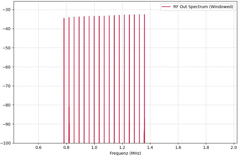
- Mediumwave (1.25 Msps): A dense synthetic 17-carrier AM broadcast band (783 kHz through 1359 kHz, spanning vintage German and dance-music and news recordings) shows sharp, symmetric carriers with no visible central LO spike — direct visual confirmation that the NCO/mixer combination achieves clean carrier suppression under a genuinely crowded multi-signal load.
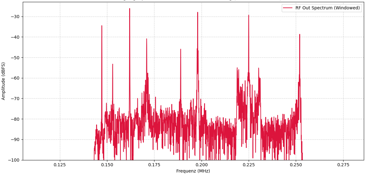
- Longwave: Real captures of actual LW broadcasters — DDH47 meteo/FSK from Pinneberg, France's TDF time signal on 162 kHz, BBC Radio 4 on 198 kHz, and others
- 49 m shortwave: Genuine ionospheric shortwave signals
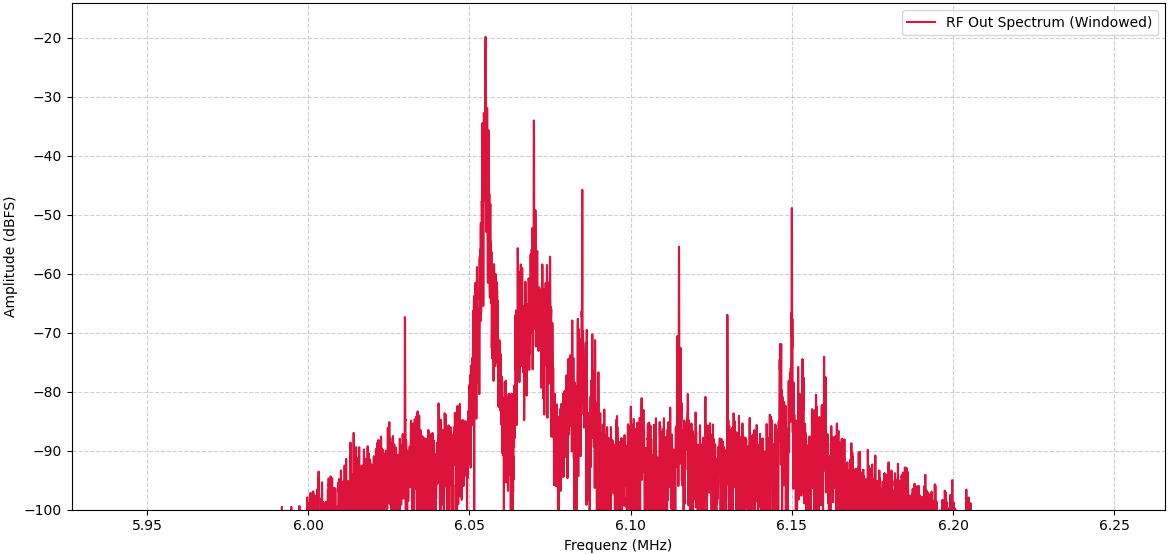
Using historical broadcast material rather than synthetic single-tone test signals is a smart verification choice: single tones flatter almost any DUC design, while a crowded, high-PAPR real-world band is where rounding errors, CIC droop, and LO leakage actually show up.
5. What This Means for the "Budget Red Pitaya" Roadmap
Looking back at Part 1's closing speculation, this release answers most of the open questions directly:
| Roadmap Item (Part 1) | Status After This Release |
|---|---|
| FPGA between parallel bus and RF front-end | Delivered — generalized Verilog core, tested on Cyclone IV/10, Lattice, and Gowin Tang Nano/Primer boards |
| Hardware-level DUC | Delivered and hardware-verified, including real-broadcast spectral validation |
| Hardware-level DDC | Architecturally present in the block diagram (ADC → DDC → RX I/Q path), but not yet implemented — the natural next milestone |
| Reversible, bidirectional DMA-to-parallel architecture | Confirmed by design intent; the shared NCO and symmetric block diagram are explicitly built to support both directions |
| Low pin-count control alongside high-speed data | Solved via the in-band 2-bit tag scheme, avoiding a second control bus entirely |
What remains open is the DDC counterpart: a receive-side decimator/mixer chain that would take a wideband ADC feed, mix it down, and decimate it back to the same 250 ksps–1.25 Msps range the DUC accepts on transmit. Given that the shared sine ROM and NCO are explicitly designed as a "dual" module and the top-level architecture diagram already draws the ADC/DDC signal path, that piece looks less like a hypothetical and more like a matter of time.
If and when that arrives, the combination of a Raspberry Pi 4 or ESP32-P4, a sub-$30 FPGA board, and a pair of parallel-bus ADC/DAC ICs will genuinely tick every architectural box that defines a Red Pitaya-class instrument: host connectivity, wideband data acquisition, and on-chip DDC/DUC — at a bill of materials that a Red Pitaya doesn't come close to matching. For educational labs, amateur radio operators, and makers who have been priced out of "real" SDR hardware, that is precisely the gap this ecosystem set out to bridge.