 Leo5593

I recently created a PCB with JLCPCB, using EasyEDA for the design. I wonder about PCB assembly possibility so give it a try.
Based on the information of pocketbeagle-2-ethernet-gigabit-cap-over-rgmii2 I start with the projects file in the git and done some adjustments to match the project criteria:
- BeagleBone Black size
- 1G Ethernet
- POE Support
One of the main concern, as mention in the forum, is the equal length for RGMII signals and also the differentials pair between the Phy and the RJ45 MagJack. Each placement change meant the rework of the length check of the RGMII signals. So let's place components first and do the routing later.
I don't have any experience on implementing a gigabit Ethernet Phy with POE, so I relied heavily on the BeagleY-AI repository and also TI Phy design layout.
The selected parts are:
- Phy DP83867CRRGZR, smallest footprint and lower price
- RJ45 MagJack, LPJG0926HENLS4R
- Use thru-hole support for the PocketBeagle 2
This selection makes obvious that the routing need to be done from the start.
Placing all decoupling capacitor with the QFN48 footprint is challenging. When done, it's to give a try to the PCB Assembly to check what would be the cost.
There is so many options, long story short, the economic assembly needs all the parts on the top or the bottom and components minimum package size is 0402. With the integration between EasyEDA and JLCPCB the components need to be chosen carefully so all the parts have their manufacturer part code and with the correct resistor or capacitor value integrated directly on the BOM. For the economic assembly there are the basic parts and the extended ones. The basic parts are commonly used and the extended have an extra fee to load the reel into the pick and place machine.
I replace the 0201 packaging to 0402 form the reference design I used, in order to comply to the assembly requirement and select basic part from JLCBPCB catalog.
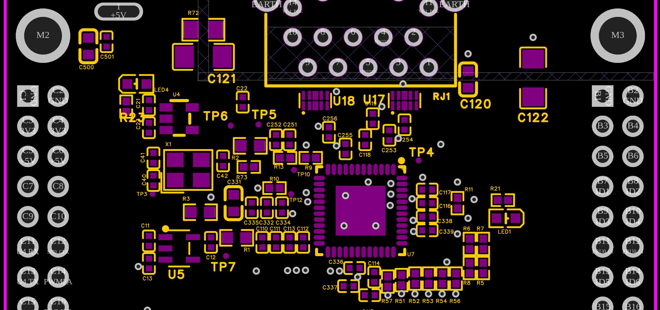
And now the fun part, the rgmii routing with same length for each 6 RX and 6 TX signal. Thanks to the information provided by Sam_Mug the missing length is take into account by adding equal length turning.
By Murphy's law the longer signal on the PocketBeagle 2 side has also the farther away on the cape. But thankfully the total length is below the 6000 mils of TI's checklist.
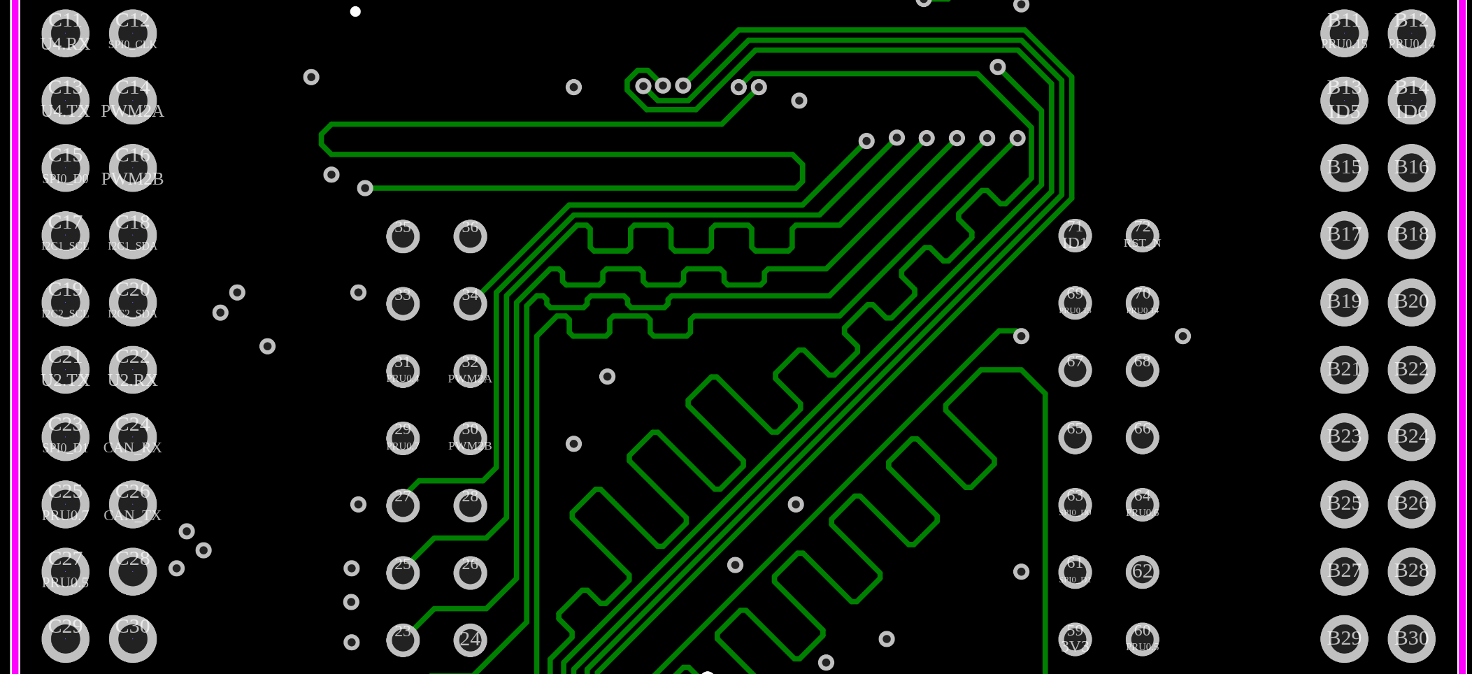
This look like a big mess but the math needs it. I wish the tool could have done it more curved but it is that it is.
Next come checking, the DRC tools has a lot of false complains but doesn't show the real one. I ask a former colleague and my brother to review it. There was missing pull-ups on the mdio and the phy reset, The USB signals need to be a differential ones. Well some details but important ones that I have would regret not correcting.
Having Ethernet is nice but the aim is to work with previous capes, this is the list of other signal connected to the P9 and P8 header of the BeagleBone Black:
- 8 GPIOS
- Also PWM0 pin A&B, UART3, UART6
- I2C2, I2C3
- UART2, UART4
- CAN0
- PWM2 pin A&B
- EQEP0 pin A&B
- SPI0
- 10 PRU0 GPIO output
As result almost all the PocketBeagle 2 expansion header are connected :
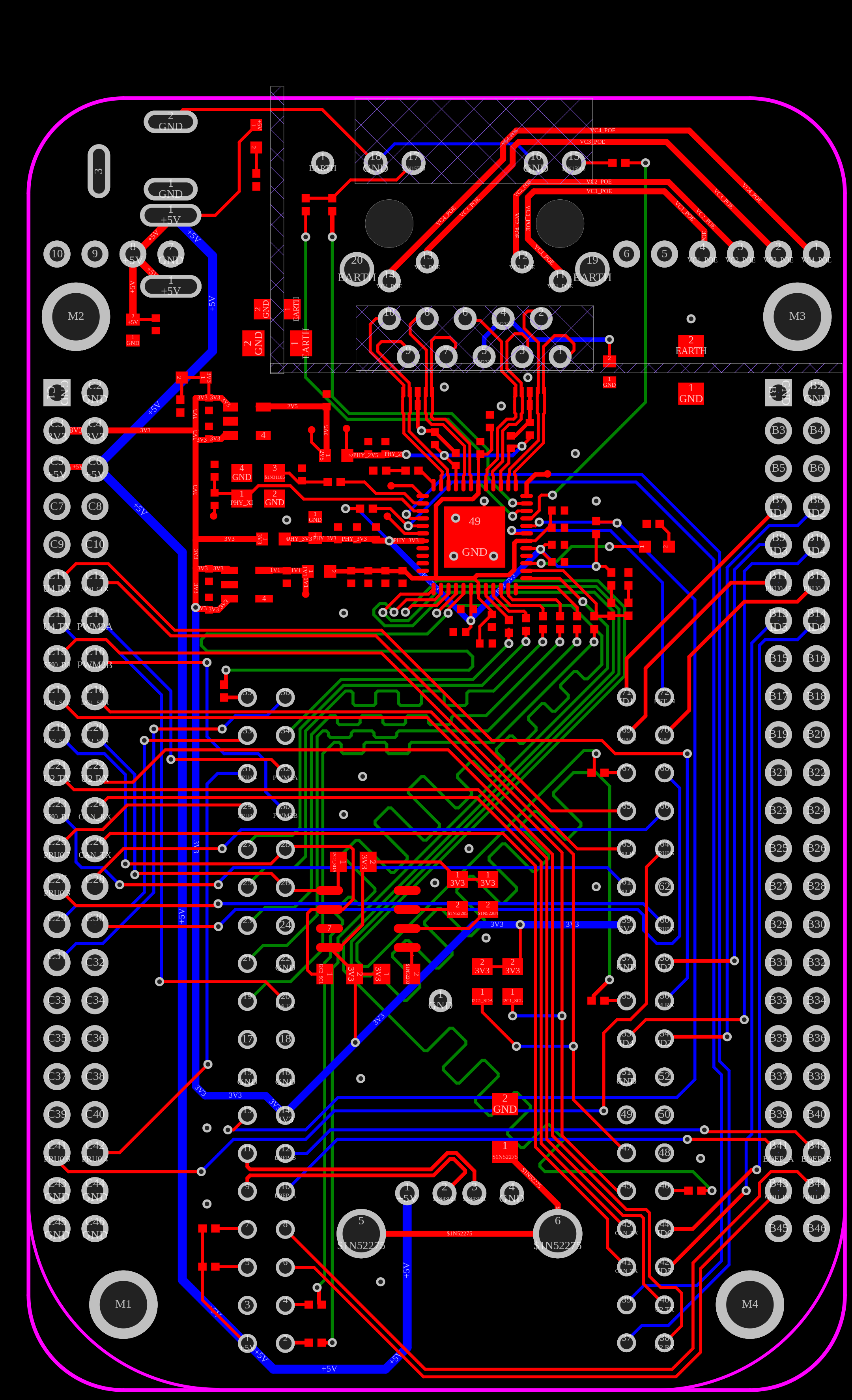
We are almost ready to order the assembly, but more checks are needed, like DFM. This check made me adjust via placement, track and component proximity. Some errors are the rgmii lines but need adjustment any way.
It is order time :
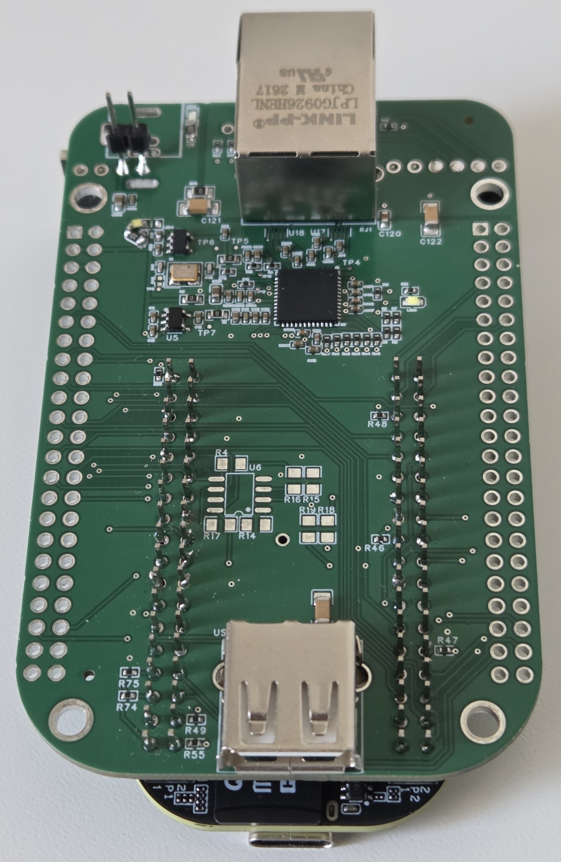
To avoid additional manual soldering cost, I sourced the thru-hole components, RJ45 MagJack and POE converter, separately. Soldering the ground pin on the header was a pain because wrong value on the spoke spacing for thermal gap.
Minor issue are reveled during testing, like the 3,3v LED not working because of an short circuit. Overall the validation came out with the PHY consuming 130mA on the 3.3v so within the 450mW matching the specification.
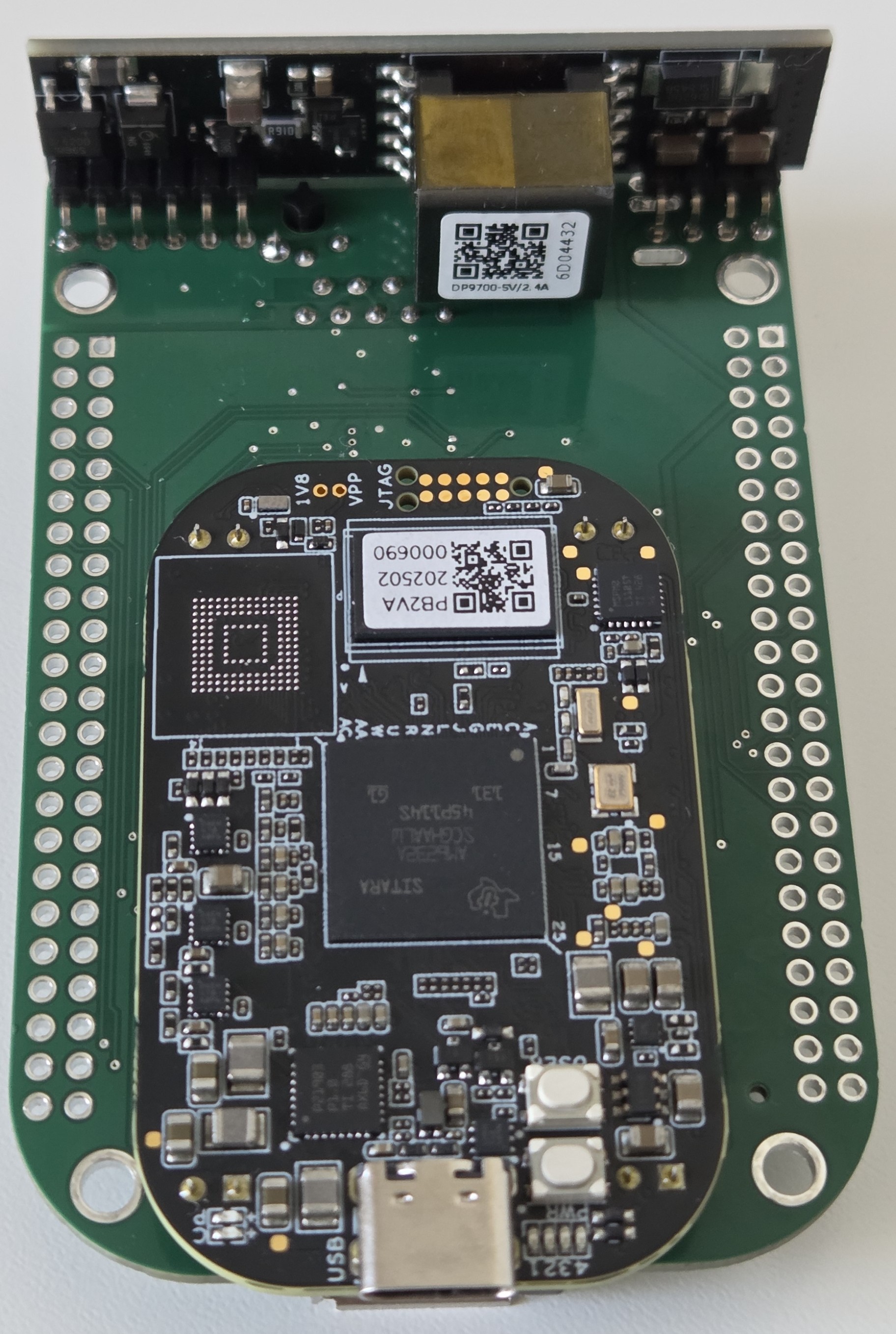
The PocketBeagle is now connected and with the devicetree overlay to enable the PHY. Once booted the PHY is detected...
Read more »
 Vini's Lab
 even_notodd
 Mastro Gippo
 Phil Weasel