Close
0%
0%

64 channel modular eeg

modular 64 channeled eeg system using TI ADS1299

Similar projects worth following
We’re building a modular 64-channel EEG data-acquisition system from scratch. The goal is to capture tiny electrical signals from the brain and send clean, synchronized data to a computer for viewing and analysis.
Each module uses eight ADS1299 chips for 64 channels, along with an FPGA to collect, organize, and transmit the data. We’re designing the analog, digital, power, and interface boards ourselves, with the idea that multiple modules could eventually be connected for even more channels.
Right now, we’ve completed much of the hardware design, tested communication with an ADS1299, established a working link between the STM32 controller and FPGA, and started testing Ethernet transmission. Our next milestone is a complete demonstration using safe test signals, with reliable data streaming, recording, and live waveform visualization.

This project is a modular EEG acquisition system designed around the TI ADS1299, a low-noise, 24-bit analog front end made for biopotential measurements.

One module will provide 64 channels using eight ADS1299 chips. An FPGA collects the channels in parallel, keeps the samples synchronized, buffers the data, and prepares it for transmission to a computer. An STM32 microcontroller handles system control, board monitoring, and communication with the FPGA.

The hardware is split across separate analog, digital, power, and user-interface boards. This makes each part easier to test and allows the system to grow by connecting multiple modules. Our long-term target is a 256-channel setup made from four synchronized 64-channel modules.

The project is currently in the hardware bring-up stage. Initial digital and power boards have arrived, STM32-to-FPGA communication has been tested, and the first analog board will initially be assembled with one ADS1299 before expanding to all eight devices.

This is an experimental research and educational platform. Early testing is being performed only with safe test signals and shorted inputs—not with human subjects.
  • The Analog Board is here, and the master enclosure is printed

    Aditya56h • 5 days ago • 0 comments

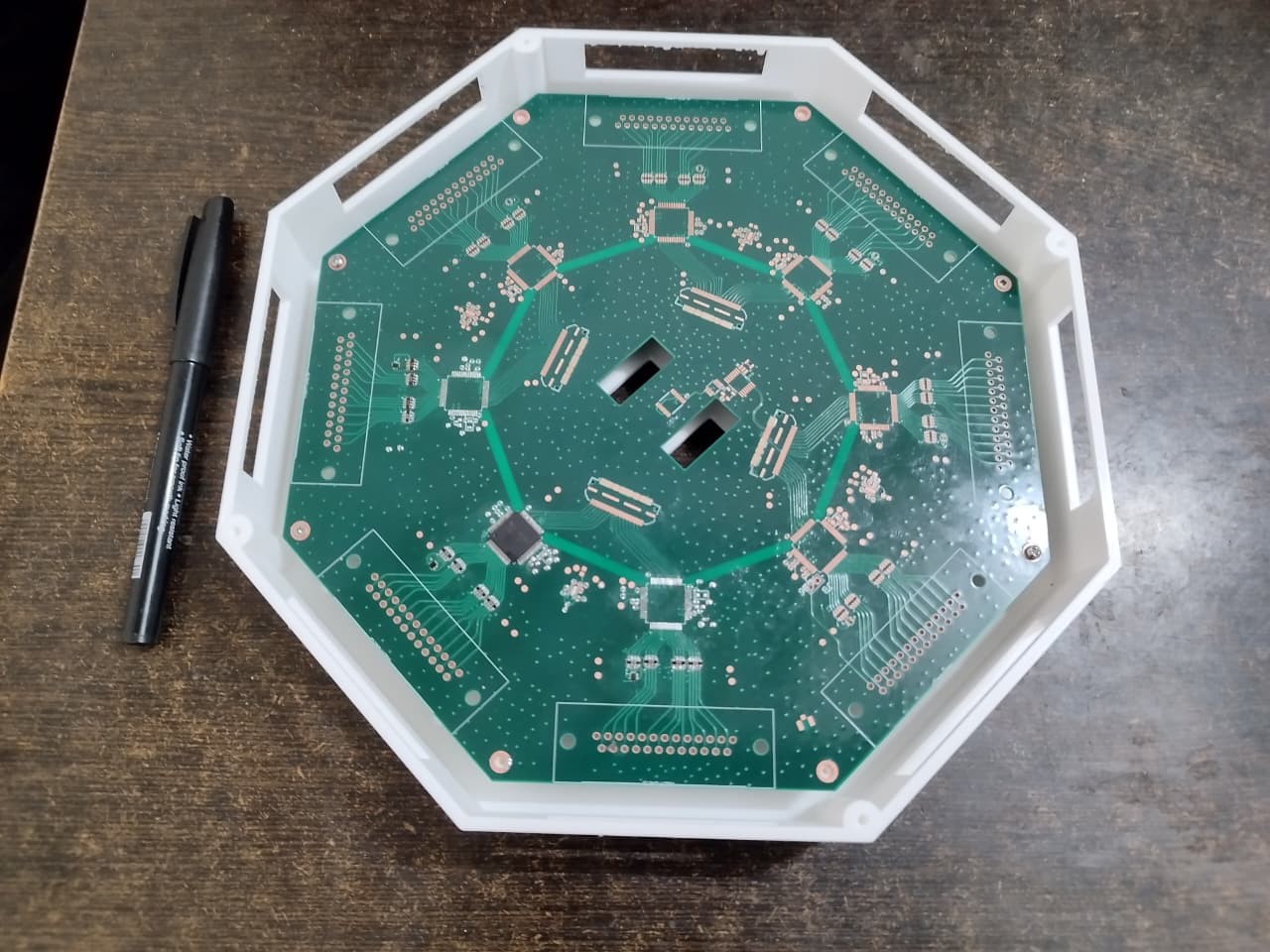
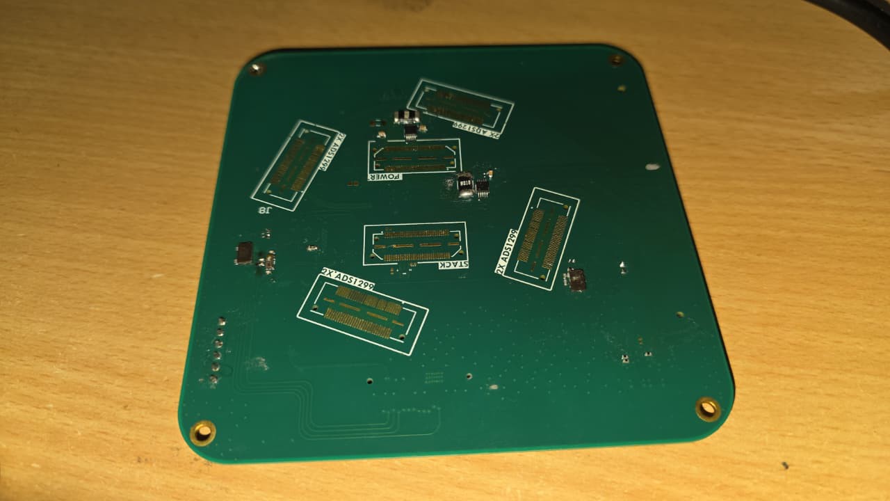
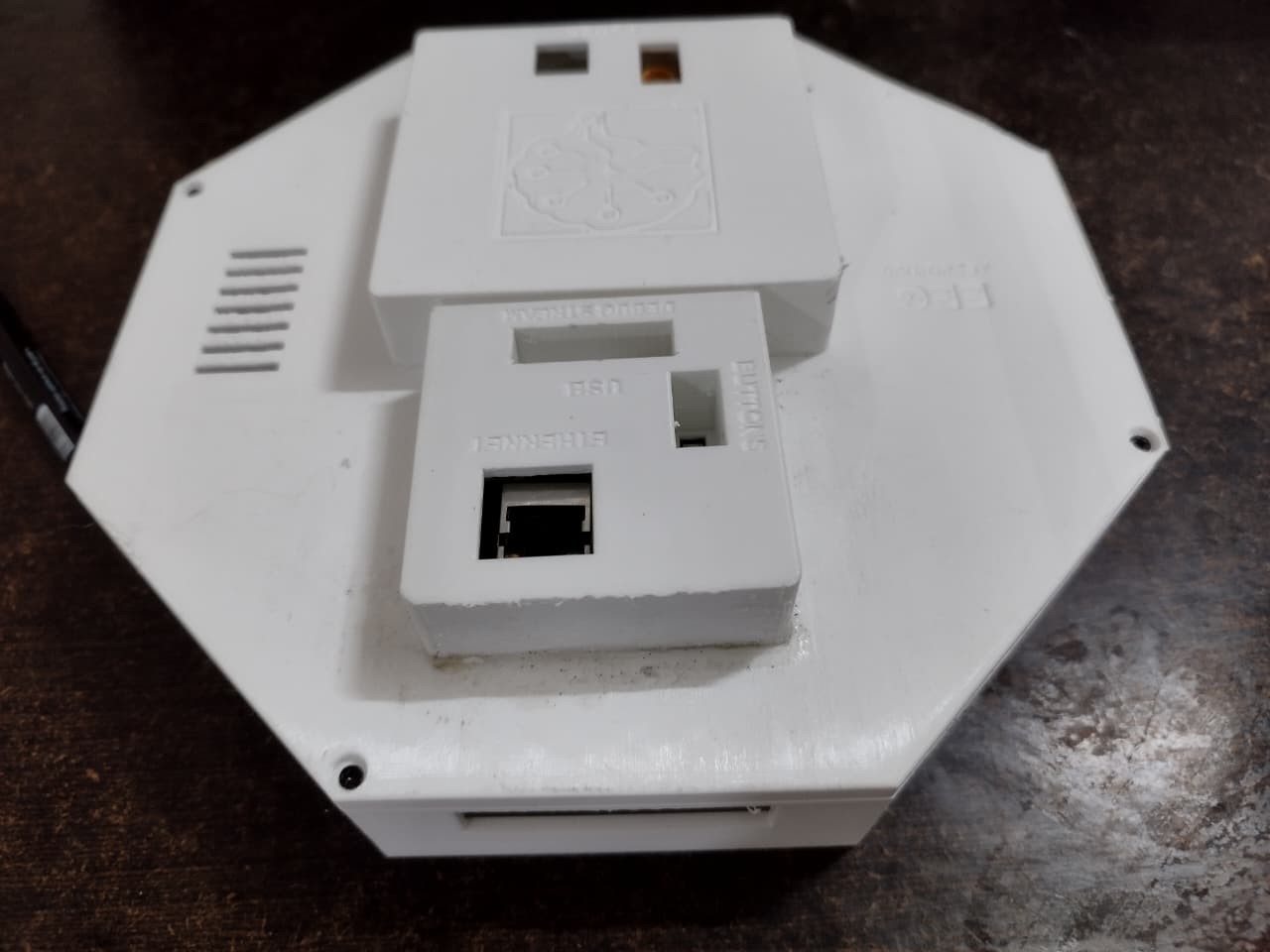
    The custom Analog Board has arrived from JLCPCB, and we have now printed the complete two-piece enclosure for the master module. This is the first time the large octagonal board and the full-size printed case can be checked together as physical parts rather than CAD geometry.

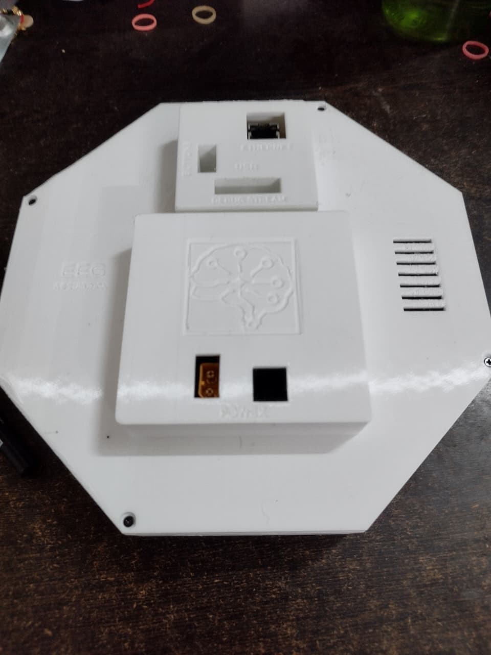
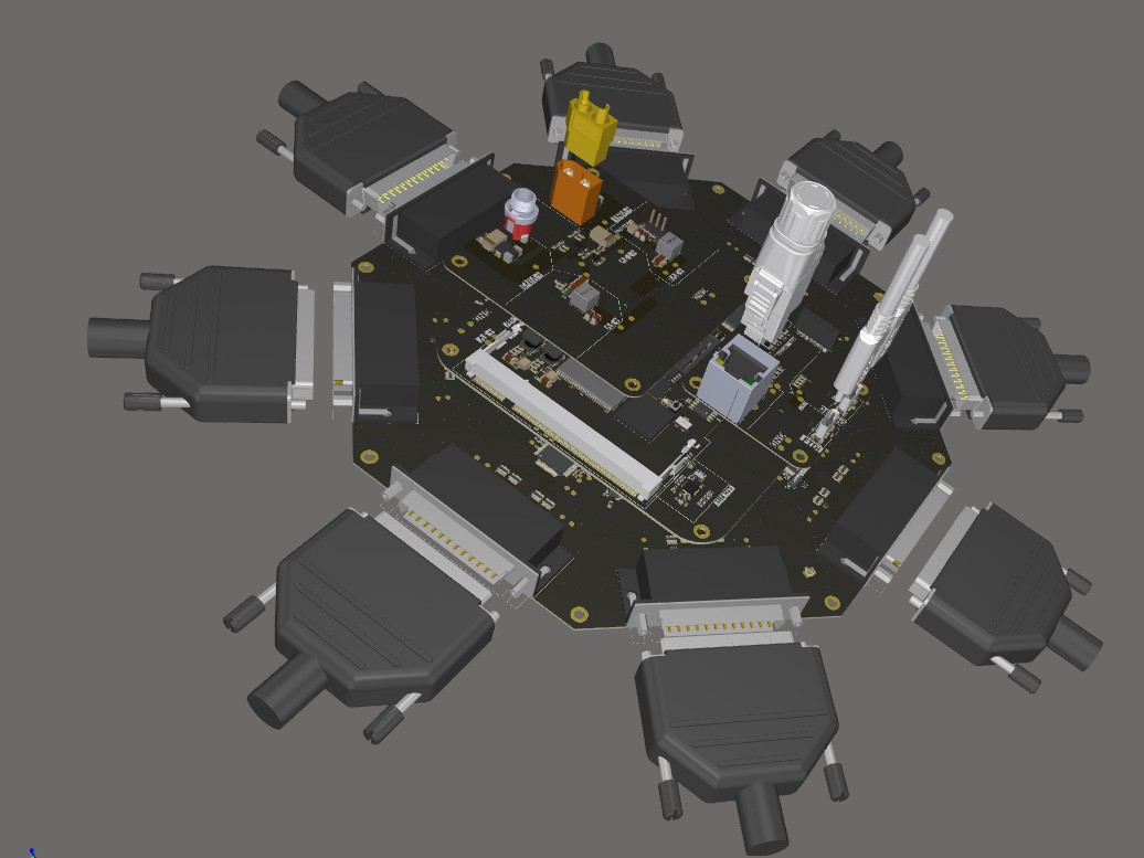
    The Analog Board sits in the lower half of the enclosure. Its eight radial connector positions run around the perimeter, while the central openings leave room for the vertical connections to the upper electronics. The new photos also show the underside of the printed case and the exterior lid, including the raised interface area, ventilation slots and recessed circuit-brain graphic. The print gives us a useful real-world check of the board footprint, mounting locations and access openings.

    We are deliberately populating the analog electronics in stages. **One ADS1299 is installed right now.** That device represents the first eight-channel section of the planned 64-channel Analog Board; the other seven converter positions will be populated later. Having one chip installed is an assembly milestone, not a claim that eight EEG channels have already passed acquisition tests.

    The immediate electrical goal is to validate this first ADS1299 path: check its supply rails, clock and reference, read its device ID, confirm register write/readback, then capture internal test and a known differential input. In parallel, we need to check the mechanical details that CAD cannot settle on its own: connector mating travel, DB25 cable and backshell clearance, fastener engagement and how cleanly the upper stack closes into the case.

    It is exciting to have both the actual analog PCB and the full master-module print on the bench. The next update will focus on measured bring-up results from the single populated converter, and then we can decide when to populate the rest of the board.

  • Building the ADC test workflow with ADS1296

    Aditya56h • 09/20/2026 at 05:54 • 0 comments

    Work date:15–16 September 2026  

    While the custom Analog Board is prepared for its first ADS1299, we have been building the acquisition and measurement workflow around a separate ADS1296 test board.

    The original ADS1299 test device failed, so the ADS1296 currently provides a practical way to debug startup timing, SPI transactions, DRDY handling, sample framing, serial transfer and analysis tools. It has six channels instead of eight, and its converter frame is 21 bytes instead of the ADS1299's 27-byte frame. ADS1299 register settings, scaling and noise results will therefore be repeated on the real target hardware.

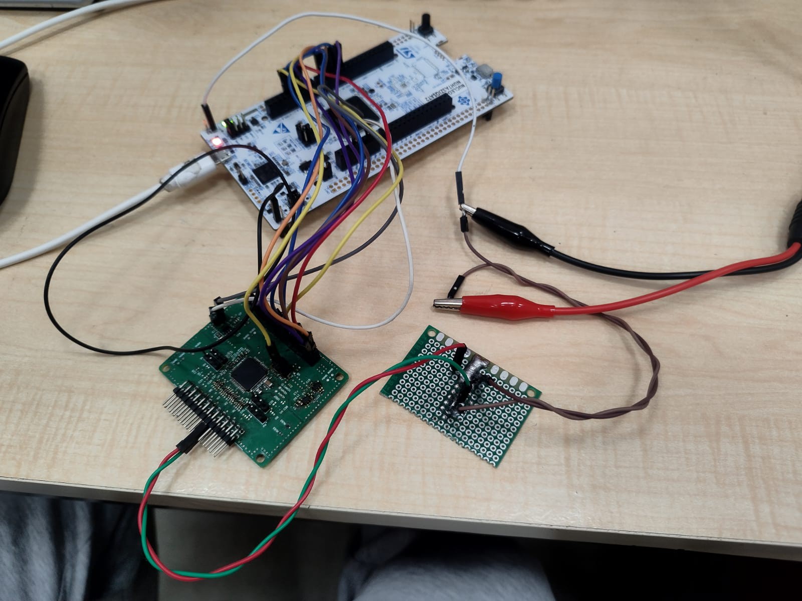
    The test board connects to an STM32 NUCLEO-H7A3ZI-Q. Current controlled captures use a 2.048 MHz external clock, 2 kSPS data rate and the converter's internal 4 V reference. A 47 kΩ/49.9 Ω divider reduces the function-generator output to a microvolt-level differential input.

    The firmware verifies the device identity and configuration registers before capture. Saved samples retain the channel number, sequence, status, gain, reference, raw code and calculated input voltage. We are recording both internally shorted channels and known sine inputs, including 5 Hz, 10 Hz and 40 Hz tests.

    The all-channel internal-short captures give a useful comparison between gain settings. At gain 12, the six mean-centered traces measured approximately 0.842–0.912 µV AC RMS during this capture. At gain 1, the six values were approximately 4.093–4.296 µV AC RMS. These are ADS1296 test-platform results under the recorded bench conditions, not final ADS1299 or complete-system noise figures.

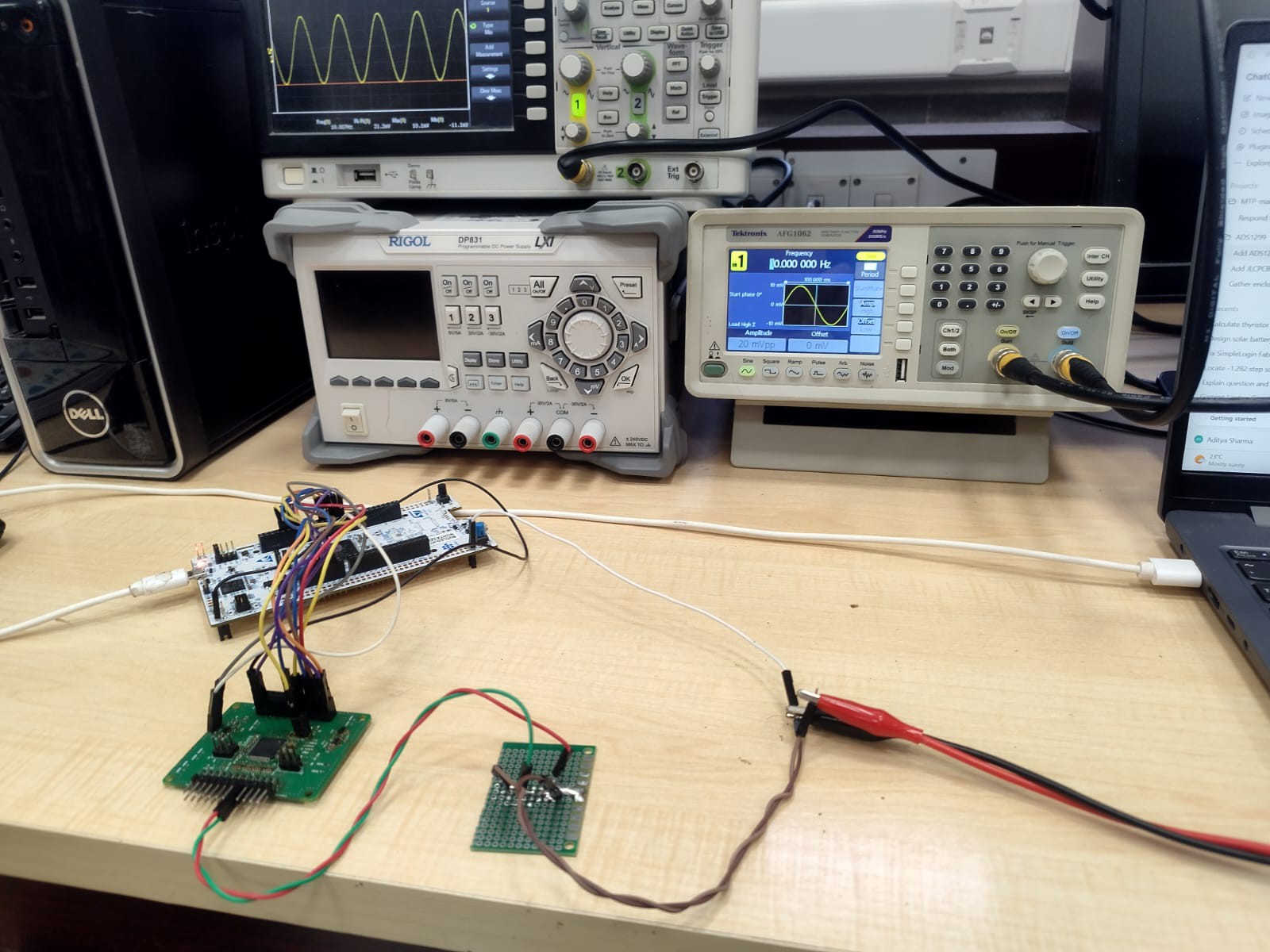
    Known-input tests used the resistor divider to translate generator settings into microvolt-level differential signals. With a 4 mVpp generator setting, the ideal divider output is approximately 4.24 µVpp. The gain-12 Channel 3 capture shows the injected tone near 9.9 Hz together with an observed 49.8 Hz mains component. A zero-phase 15 Hz low-pass view retains the test tone while reducing the 50 Hz region for analysis.

    A second test used 10 mVpp at a nominal 10 Hz, corresponding to approximately 10.6 µVpp ideally at the converter input. The raw plot keeps the approximately −610.9 µV DC baseline separate from the mean-centered AC view. The filtered time trace and Welch PSD make the 10 Hz response visible while showing the effect of the 15 Hz analysis filter.

    The raw captures remain the measurement record. The filtered traces are analysis views and are not being presented as a change to the converter data.

    Filtered time-series view preserving the injected 10 Hz waveform.

    Welch PSD for the 10 mVpp/10 Hz test, with full-range and passband detail.
    Channel 3, 4 mVpp generator setting and gain 12: raw versus zero-phase 15 Hz low-pass
    Welch PSD for the 4 mVpp test, showing the 9.85 Hz injected tone and 49.8 Hz mains peak.
    STM32 NUCLEO, converter PCB and divider/interface wiring.
    ADS1296 known-input test with function generator and oscilloscope.”
    All six channels internally shorted at gain 12; approximately 0.842–0.912 µV AC RMS in this capture.

  • more cad stuff

    Aditya56h • 09/20/2026 at 05:35 • 0 comments

    Work date:14 September 2026  

    The enclosure work has expanded from one 64-channel unit into a mechanical plan for multiple synchronized modules.

    There are

    two different uses of the word “master” in this project. Inside one Analog Board, the eight ADS1299 devices use one master and seven slaves in the analog bias/reference topology. At enclosure level, a master module and slave modules describe complete 64-channel units. These are separate relationships.

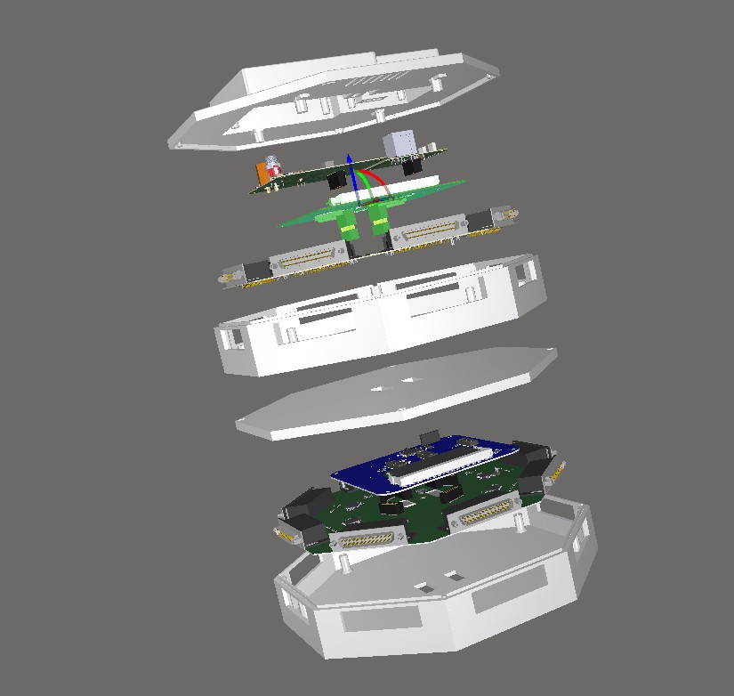
    The **master module** contains all four PCBs:

    - Analog Board;
    - Digital EEG Board;
    - Top Power Board;
    - Top I/O Board.

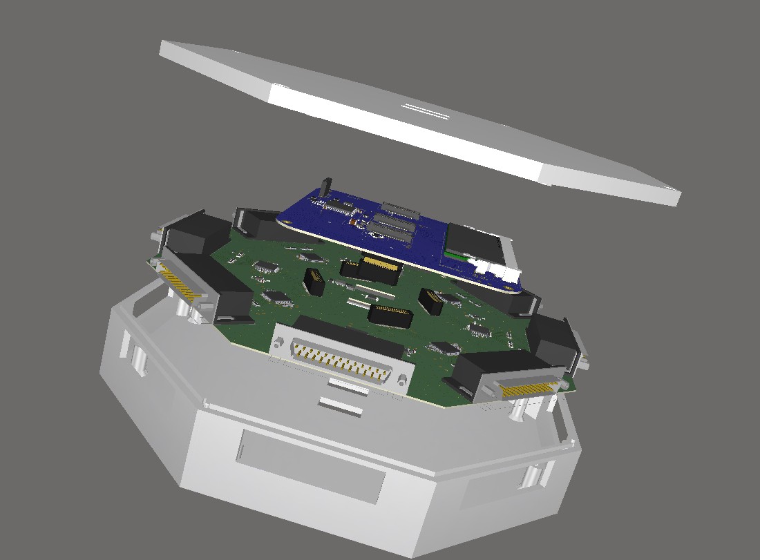
    A **slave module** contains its own Analog Board and Digital EEG Board but does not duplicate the Top Power or Top I/O boards. Its lid is therefore simpler and only needs the mechanical and vertical-stack passages required by the digital interconnect.

    The first multi-module target is one master plus one slave, which gives a 128-channel design capacity. After timing and data transport work with two modules, the long-term target is one master plus three slaves for 256 channels.

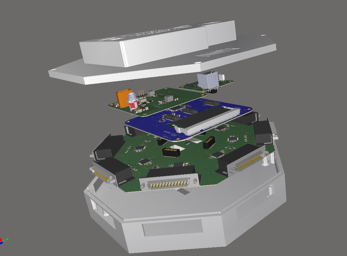
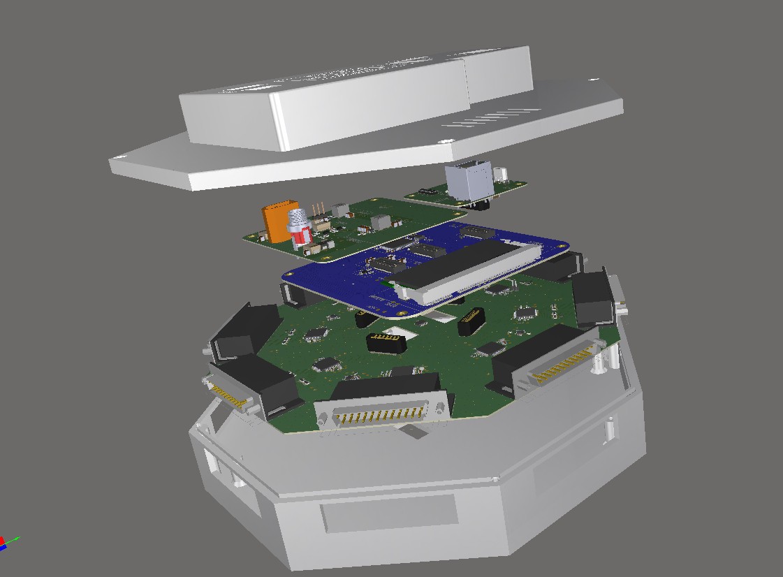
    The exploded CAD views are useful for checking the intended order, but the multi-module electrical links and synchronization have not yet been demonstrated. The next meaningful result will be a shared timing and data test between two physical modules, not simply a larger rendered stack.

    One-master/one-slave arrangement, the first 128-channel expansion target.
    Slave module with Analog and Digital EEG boards and a plain lid

  • enclosure design stuff

    Aditya56h • 09/20/2026 at 05:29 • 0 comments

    Work date:12–13 September 2026  

    The original Altium assembly STEP was approximately 123 MB and contained far more detail than an enclosure needs. Individual resistor, capacitor and IC models made the file heavy without improving the mechanical result. We simplified the assembly while retaining the geometry that controls fit:

    - PCB outlines and thickness references;
    - mounting-hole locations;
    - DB25 bodies and access directions;
    - vertical board-to-board connectors;
    - external USB, Ethernet and button locations;
    - conservative component-height envelopes.

    The resulting enclosure uses two printed pieces and measures approximately 221 × 221 × 61.5 mm. The octagonal Analog Board sits in the bottom. The Digital EEG, Top Power and Top I/O boards attach to the lid and lower vertically onto the analog section.

    Master enclosure exploded view with the four-board stack

    full assembly cad from earlier

  • The upper digital stack powers up

    Aditya56h • 09/20/2026 at 05:24 • 0 comments

    Work date:** 8 September 2026 

    The three upper PCBs have now been assembled into the first practical digital stack.

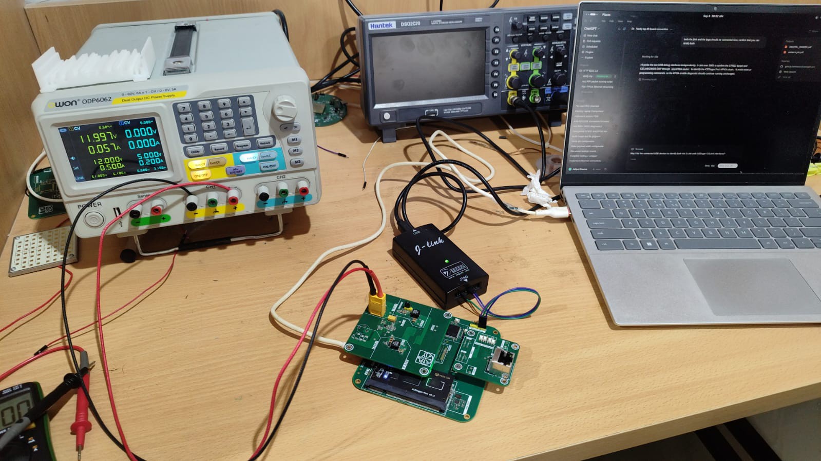
    The setup uses a current-limited laboratory supply, J-Link for STM32 debugging and USB access to the iCESugar Pro FPGA module. This arrangement lets us inspect each layer while keeping the Analog Board disconnected.

    During bring-up we checked the important power and reset conditions. The FPGA core domain measured near 1.2 V, the I/O domain measured near 3.3 V and the PHY reset signal was active. A short involving two pins was also identified and corrected. The STM32 and FPGA communication path was exercised after the correction.

    This is useful progress, but it is still board-level bring-up. A powered Ethernet connector and healthy reset level do not prove that the PHY can identify correctly, establish a cable link or transfer packets. Those checks will be retained as a separate milestone with MDIO register evidence, link status and captured traffic.

    The assembled hardware is also providing the first reliable physical reference for the enclosure. The real board outline, mounting holes, connector heights and cable directions matter more than the approximate component placement in the original assembly export.

    Assembled upper stack under current-limited bench power.

    Close-up of the Top Power, Top I/O and Digital EEG assembly

  • basic pcb testing stuff

    Aditya56h • 08/26/2026 at 17:16 • 0 comments

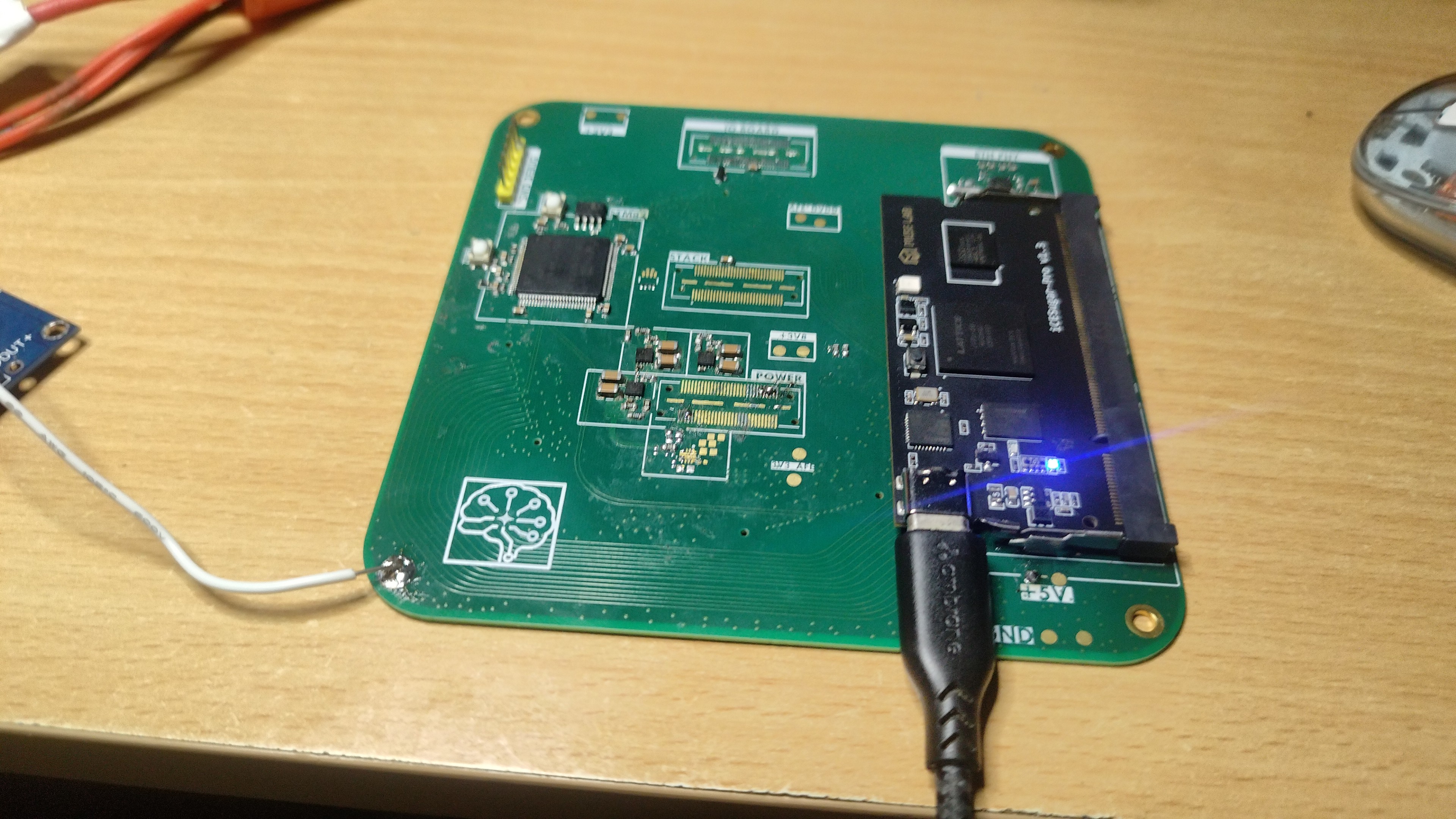
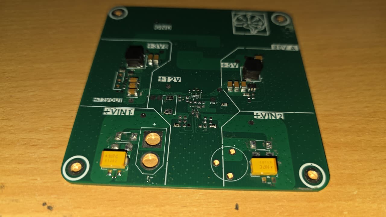
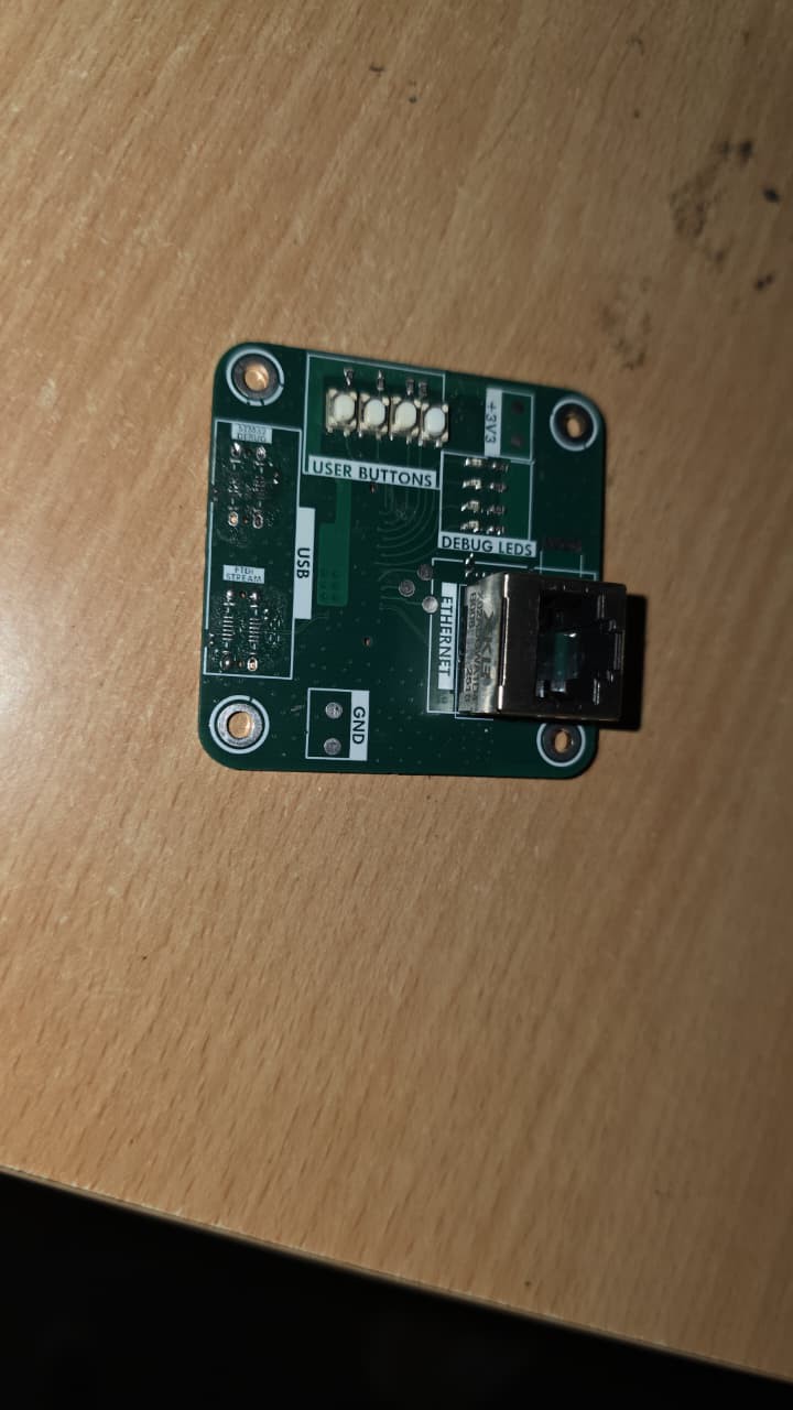
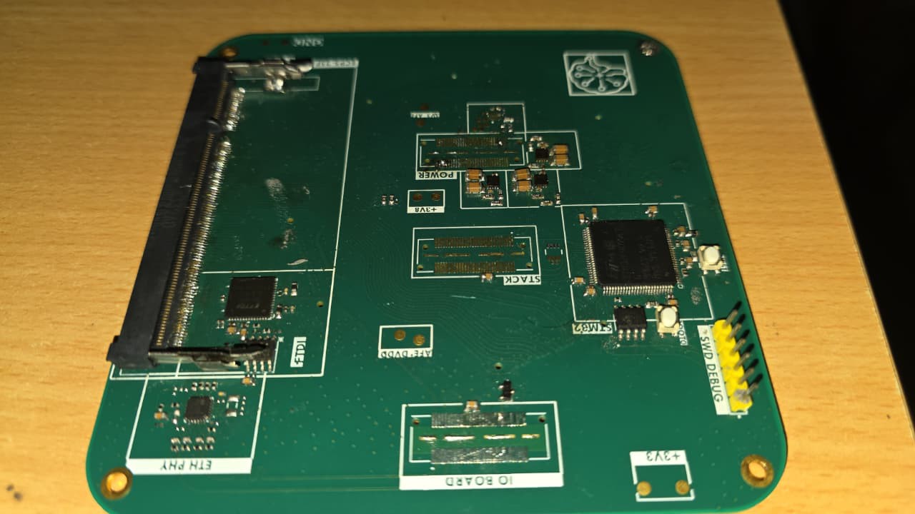
    the ordered pcbs for the digital control part and power stuff has arrived the fpga and stm32 link was tested and is good the power board stuff works too the board  to board  interconnects havent arrived will update  with all three boards working together after that the analog board will be ordered by  5th september with its components  no issues wer found in current board desgins till now i am using icesugar pro fpga boards for now . the analog board will currently only house one TI ADS1299  only on its sucessful test will the other 7 be ordered .  the whole system will be modular with upto 256 channels as my future target for that the current pcbs have inter  module connectors too but these will be tested once the tests for single module operations have been finished

    power input board
    efuse will arrive in a few days
    IO board
    will be used after the board to board connectors arrive to me
    digital control board

View all 6 project logs

Enjoy this project?

Share

Discussions

Similar Projects

Does this project spark your interest?

Become a member to follow this project and never miss any updates