Crux Resolve

I work with PLCs and industrial controls for a living. ESP32s, PCB layout, and mobile app development were definitely not my normal world when this started.
I’m comfortable troubleshooting machines, working through ladder logic, chasing I/O problems, and figuring out why something in a control system isn’t behaving. But before this project, I had never designed a PCB and sent it out to be manufactured.
This whole thing started because I wanted a better way to communicate with an aftermarket ECU.
I had a MicroSquirt running MS2/Extra that communicated over RS232, and I wanted to be able to tune it from an iPhone instead of always needing a laptop and serial cable.
The basic idea looked simple enough:
ECU → RS232 → WiFi → iPhone
It turned out that little diagram was going to make me learn a ridiculous number of new things.
Getting Outside the PLC World
My first problem was figuring out how to get from an ESP32 to actual RS232.
I knew serial communications from the industrial side, but I wasn’t building embedded hardware every day. One of the early things I had to really understand was that the UART coming out of an ESP32 is not electrically the same thing as RS232.
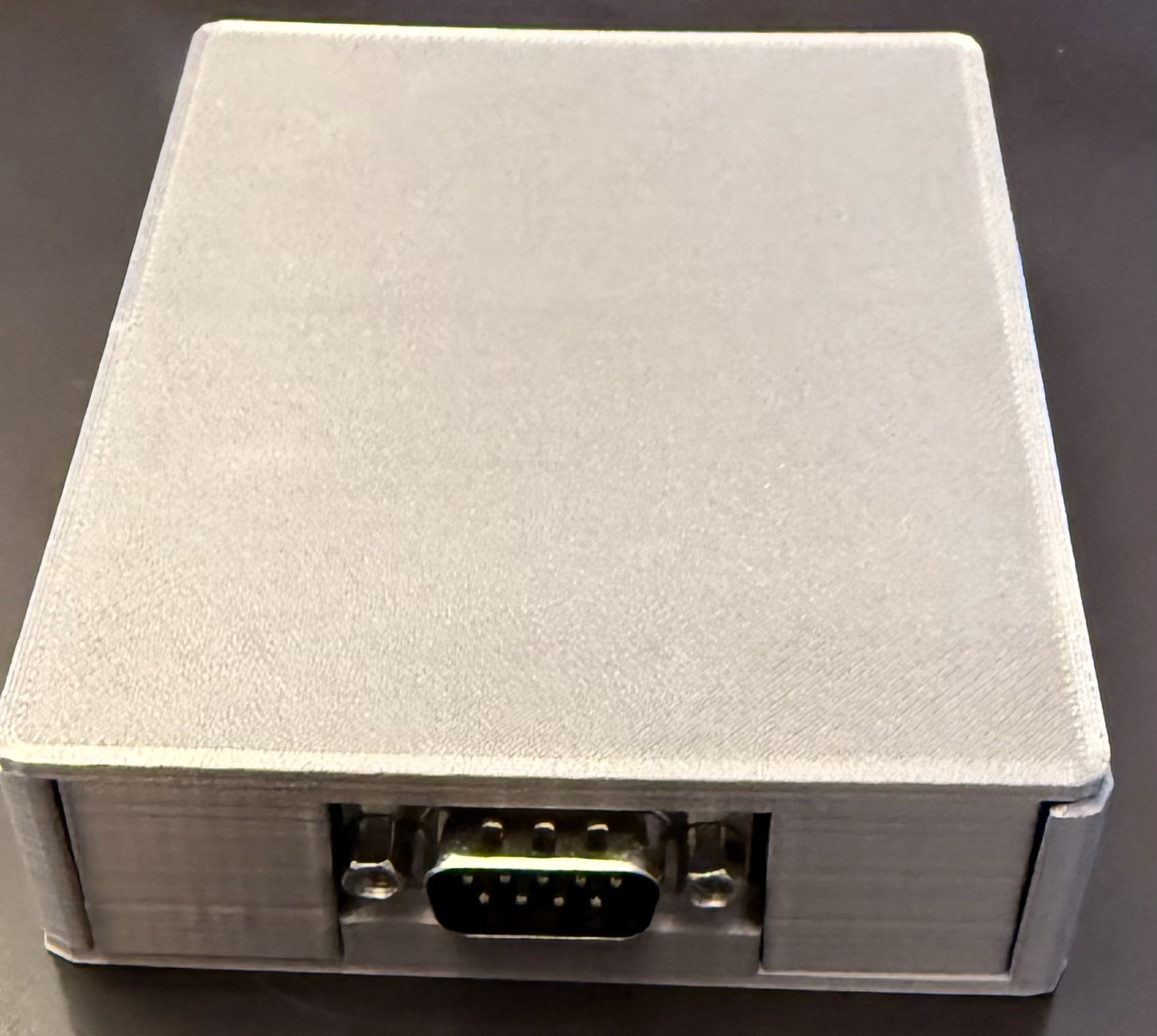
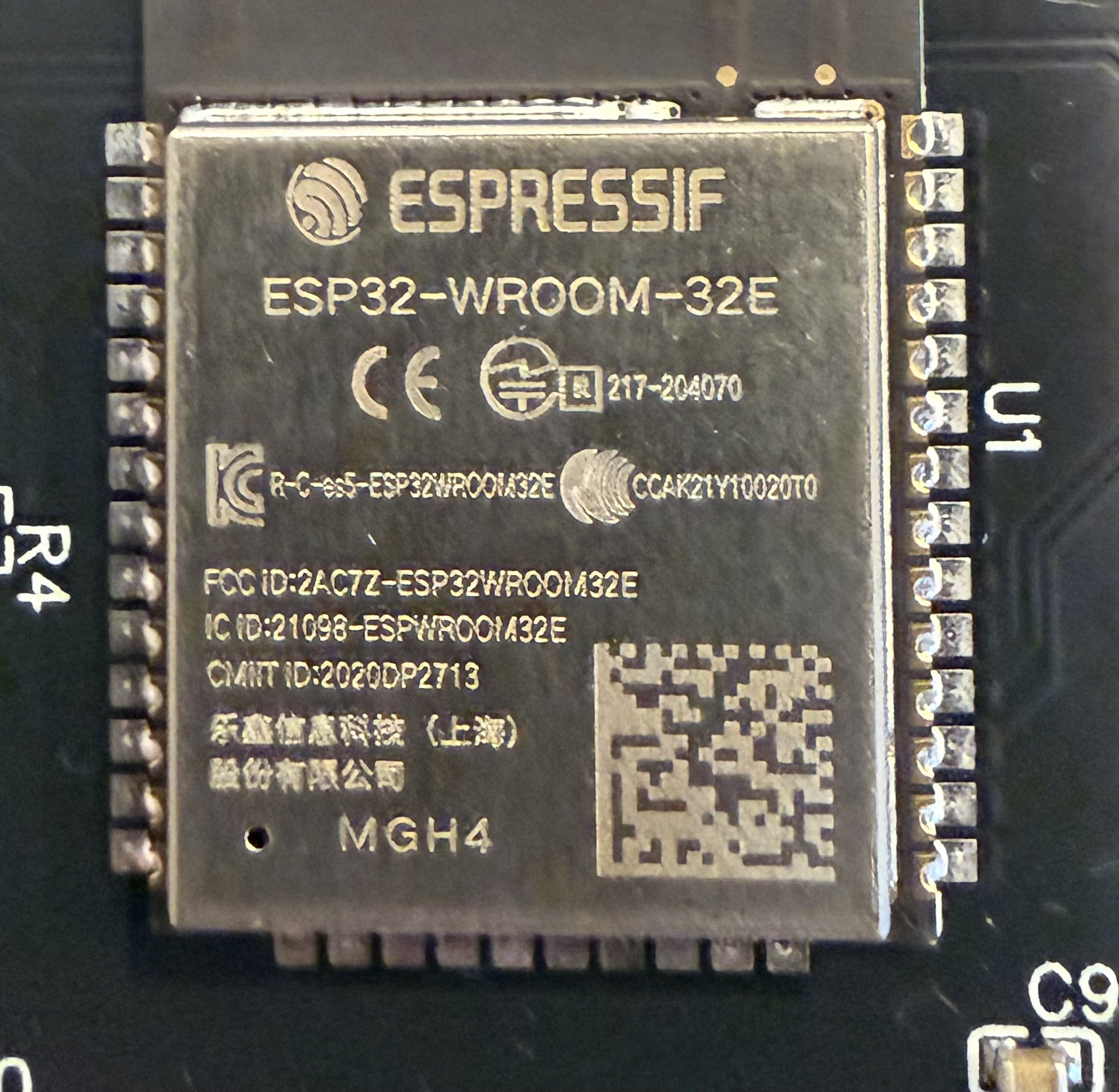
That led me to the MAX3232 and eventually to a circuit with the ESP32, RS232 transceiver, DB9 connector, USB-C power, and the supporting components around it.
The current version of the board, GB-01, uses a simple three-wire RS232 connection: TX, RX, and ground. I did not route RTS/CTS or the other modem-control signals on this version.
Looking back now, some of that seems obvious. It wasn’t obvious when I was starting.
Learning EasyEDA
Then I had to turn a circuit into an actual PCB.
The first time I started working seriously in EasyEDA, I had a lot to learn. Schematics were one thing. Footprints, net assignments, component placement, routing, board clearances, design-rule checks, connector placement, and manufacturing requirements were another.
I also learned pretty quickly that selecting a component isn’t just about whether it works electrically.
Can the manufacturer actually get it?
Is the footprint correct?
Can it be assembled?
Is there enough room around it?
Did I accidentally choose a part that makes sense on paper but creates a headache once it gets onto a board?
I spent a lot of time going back and forth between datasheets, EasyEDA, component listings, and the physical layout.
Eventually I got to the point where I could send the design to JLCPCB and have the boards professionally made and assembled.
Seeing the first real PCB show up was a pretty big moment for me. Until then, everything existed on a monitor.
Then I had something in my hand that either worked or didn’t.
Using AI While Learning All of This
AI was a big part of the process, especially because I was working outside of my normal field.
I used it over several months to help work through datasheets, component choices, schematic questions, ESP32 firmware, EasyEDA issues, PCB reviews, manufacturing questions, networking problems, application code, and eventually the enclosure.
That does not mean I asked AI to design the thing and then just sent the result off to be manufactured.
There were plenty of times when an answer sounded right and the hardware proved otherwise.
There were also plenty of times when I had to stop, pull up the datasheet, get the meter out, trace a signal, or test something on the actual board.
At some point my rule became:
The board on my bench was the final authority.
AI could help me understand something or suggest what to check next, but voltage measurements, continuity, packet tests, datasheets, and the actual hardware decided what was true.
When the Board Didn’t Behave
One of the more memorable problems was getting the serial communication path working correctly.
The ESP32 was running. The RS232 circuitry had power. I could measure about the kind of RS232-level voltage I expected on the transmit side, so the MAX3232 was clearly doing something....
Read more »