 Robert Rico
Why a third try
I had three major revisions, s8008, v8008 and finally b8008. ( My thinking was soft8008, verbose8008 and block8008. s8008 reached hardware before I understood its timing model was wrong. v8008 had too much shared logic and conditional soup to debug. b8008 started from a clean slate in November 2025 with one module per block-diagram box, and every module got its own testbench before the top level existed.
Architecture
About 27 modules, each one a box from the Intel diagram: state timing generator, machine cycle control, instruction register, instruction decoder, register and ALU control, register file, temp registers, ALU, carry look-ahead, condition flags, address stack, stack pointer, interrupt and ready flip-flops, I/O buffer, memory mux. Each is 50 to 100 lines and does one thing. The stack pointer is 69 lines and knows two words, push and pop. It has no idea what CALL or RST or an interrupt is.
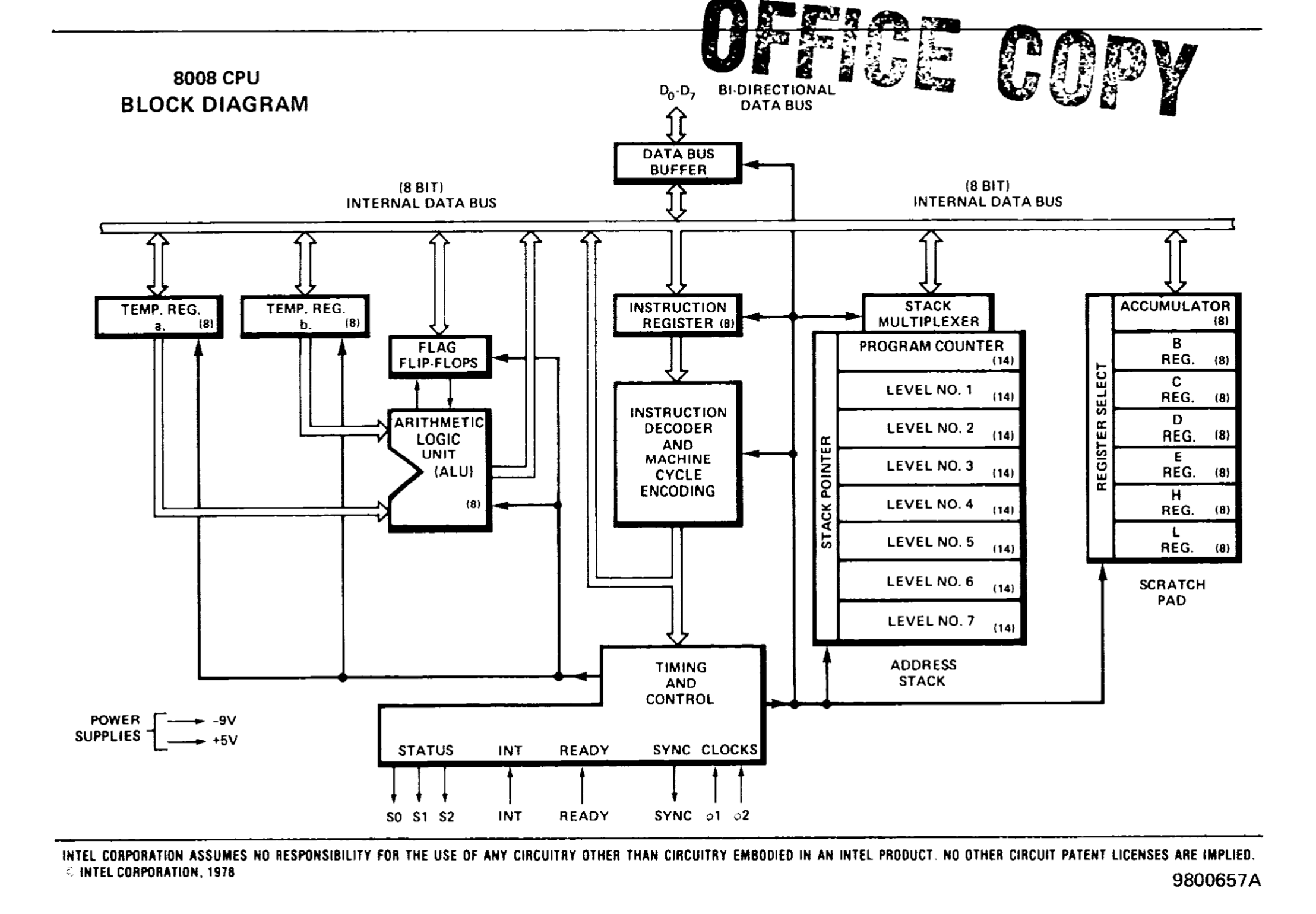
There is no separate program counter, because the real chip doesn't have one. The PC is whichever of the eight 14-bit address-stack registers the stack pointer selects. CALL is the SP moving on and the old slot keeps the return address. RET is the SP moving back. Seven nested returns, and the eighth CALL wraps onto the oldest. I built it with a separate PC first and a family of workaround flags grew around it. Rebuilding it as the diagram shows deleted all of them.
Every documented instruction takes the datasheet's 5, 8 or 11 T-states. Fetch cycles of multi-cycle instructions end at T3, not-taken conditionals end early, and a regression counts simulated states per timing class against docs/isa.json. Interrupts are recognized only at instruction boundaries, per Figure 2 of the User's Manual. READY parks the CPU in a real WAIT state between T2 and T3.
The ALU's adder is the carry look-ahead block. For a while that block compiled and had a testbench and nothing instantiated it, and the toolchain was inferring the adder from numeric_std. It's wired in now, with a 9-bit carry-out and an exhaustive sweep behind it.
The whole design runs in one 25 MHz clock domain. phi1 and phi2 are one-cycle enable pulses off a phase_clocks state machine, with the pulse widths parameterized so the 8008's 0.8 and 0.6 microsecond phases hold at any system clock. The internal bus is a mux. An early version used tri-state signals internally and they turned out to be the critical path.
Hardware
The board is a Lattice ECP5-5G Versa development kit, so there's no PCB of mine in this project. The 100 MHz oscillator goes through an on-chip PLL to 25 MHz, and everything runs on that. A T-state measures about 4.4 microseconds against the real chip's 4 at 500 kHz.
Serial is the on-board FTDI at 115200 8N1, local echo off, DEL for rubout because that's what the 1976 software expects. ROM and RAM are block RAM inside the FPGA. Firmware gets patched into the bitstream with `ecpbram` after place and route, which takes 0.66 seconds against a 4 minute resynthesis.
DIP switch 1 is reset. Switches 2 through 8 are disconnected after too many sessions where the wrong resting position halted the CPU or put the LEDs into a capture mode. The seven user LEDs show one RAM byte, bit n to LED n. LED0 is the CPU-running light.
There's a logic analyzer header carrying INT, phi1, phi2, SYNC, the three state bits and the eight data lines, with a DSView config and Python decoders in the repo for reading traces back into instruction streams.
In January 2026 I tried an AT28C64B EEPROM as external ROM, the way the SIM8-01 did it. It executed code when it booted, and boot was unreliable for months. The TXS0108E level shifters were being run past absolute maximum. ROM went back inside the FPGA.
Firmware
Toolchain is GHDL, Yosys, nextpnr-ecp5 and ecppack from OSS CAD Suite on macOS. 8008 assembly goes through the AS assembler in 8080 syntax. Everything goes through the Makefile.
b8008_monitor. ROM 4 KB at 0x0000, RAM 12 KB at 0x1000. The monitor has D (dump), W (write), L (Intel HEX load over the same serial line), G (go, through a JMP trampoline because the 8008 has no indirect jump) and H (help). Programs own 0x2000 to 0x3EFF. RST 1 through 7 vectors in ROM forward to 8-byte RAM slots at 0x3FC0 so a loaded program can install its own handlers. The hardware self-test ROM runs 46 ISA tests on the board and reports each over serial.
b8008_basic. RAM 4 KB at 0x0000, ROM 12 KB at 0x1000 holding the monitor and SCELBAL. Three bytes of block-RAM initialization at address zero, JMP 1800h, land the CPU in BASIC at power-on. MON lives in an unused zero-filled slack region of SCELBAL's keyword table and jumps to the monitor. G 1FB6 warm-enters BASIC's executive without re-initializing. SCELBAL is kept faithful to Jim Loos's build.
The two builds are the same b8008_top with the memory map as generics.
Period software that loads and runs from RAM: the SCELBI Mandelbrot renderer, the pi digit generator, HEXPAWN (1973), the SCELBI floating-point calculator (1974) and Shooting Stars from Byte, May 1976. Each port's changes are kept to the ORG, the serial shims and the exit. The 1974 calculator found five CPU bugs a 42-test self-test had missed: carry on INR/DCR, rotate flags, the WAIT state, boundary-only interrupts, and the PC living in the address stack.
Verification
Every module has machine-checked verification that runs in CI on each push. SBY property suites for eleven modules plus a composition cluster. Seven SBY miters and six EQY checks proving each module equivalent to its own Yosys write_vhdl round trip. Seven cocotb runs including a whole-system bus-protocol monitor. Exhaustive sweeps of the decoder and ALU. A 37-program regression on both the RTL and netlist cores, where every program asserts its own register state through OUT 31 checkpoints, so no test passes by not crashing. A differential fuzzer that runs random legal programs on the RTL and the round-tripped netlist under three oracles at once. Each checker was mutation-tested by planting a bug in the RTL and confirming it fails. The bus-protocol monitor caught a transposed cycle code on its first run.
Open problems
- External ROM was never made reliable. The TXS0108E shifters were the wrong part and the redesigned wiring (direct 3.3 V drive on address and control, resistor dividers on data) hasn't been built.
- The bootstrap RST-0 jam consumes one stack level for good, so programs get six safe nesting levels instead of seven. Real silicon booted the same way does the same thing.
- It has never been run side by side with a real 8008. The plan is a shifter board and a socket, and then the same programs on both.
- No removable media. SD over SPI as a modern cassette was the idea.
Elsewhere
The same core runs inside the Byte Hamr card as an 8008 coprocessor for the Apple IIe, pulled in as a FuseSoC-generated netlist, and on the network as LiteX 8008 Node, which answers make login over the LAN.
- Repo: https://github.com/robertrico/intel-8008-vhdl
- CI: https://github.com/robertrico/intel-8008-vhdl/actions/workflows/verification.yml
- Build logs: https://bytehamr.com/projects/intel-8008-vhdl/
- Build thread on VCF: https://forum.vcfed.org/index.php?threads/block-based-intel-8008-in-vhdl-seeking-fpga-advice.1255974/
- Period software source, Mike Willegal's SCELBI apps page: https://www.willegal.net/scelbi/apps8008.html