 Max.K
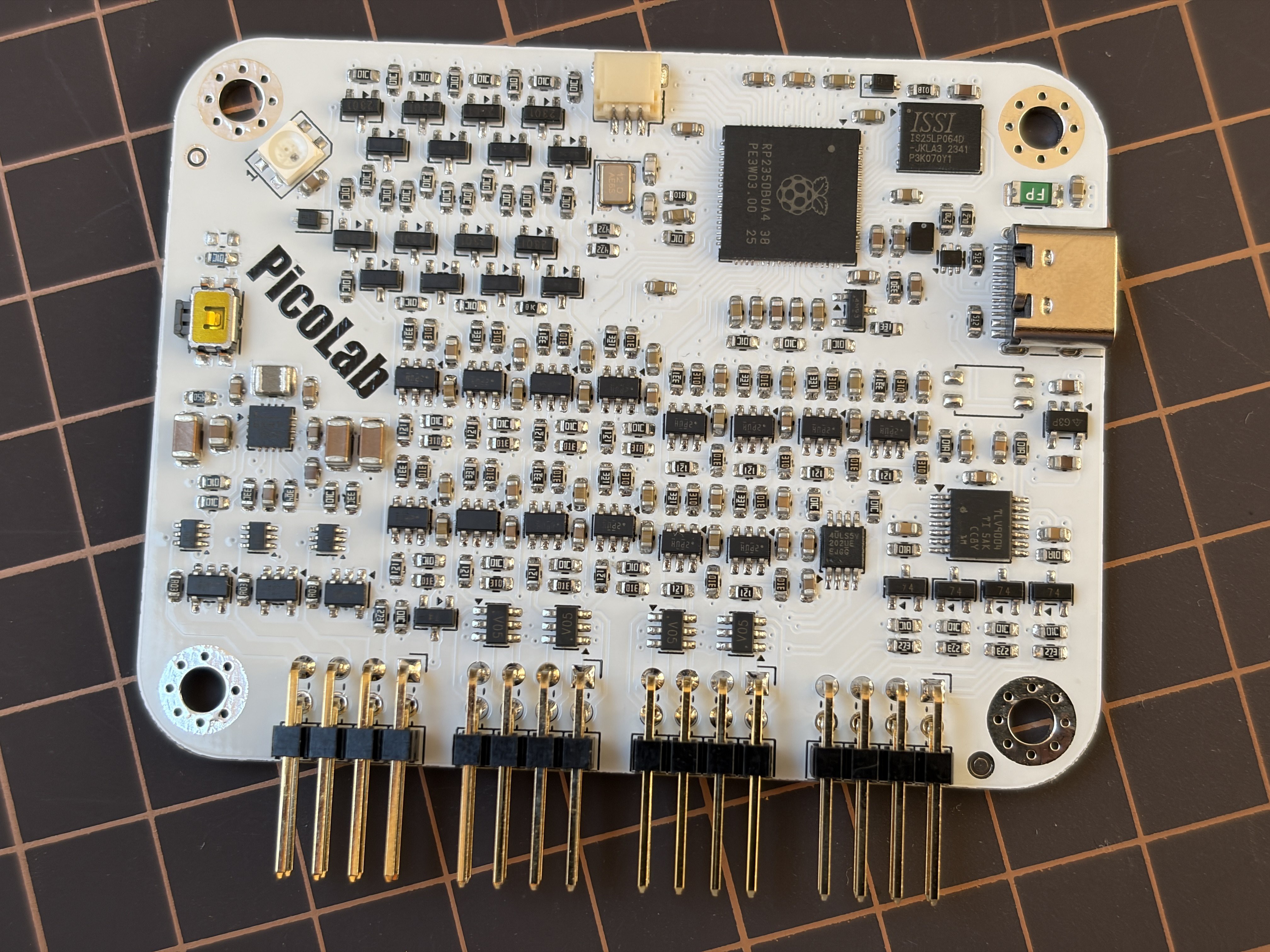
One of my main goals from the start was to make the project accessible to anyone with an off-the-shelf Raspberry Pico. The RP2040/RP2350 controllers will function perfectly well as a simple oscilloscope and logic analyzer. But these boards lack protection and work only at 3.3V. To enable the full feature-set and add some robustness, I designed a custom PCB.
For the microcontroller, I selected the RP2350B, which offers more GPIO in a 48-pin package as well as 8 ADC channels vs the 4 channels on the more common RP2350A. Half the ADCs will be used for the oscilloscope, the others for current and voltage monitoring. To make analog measurements more accurate, I added a voltage reference (LM4040) to the VRef input. The Picos usually need a button to configure them for the USB bootloader mode. I included a 90° tactile switch on the board edge for this purpose. The button is also wired to a GPIO pin, so it can be used by the firmware at runtime.
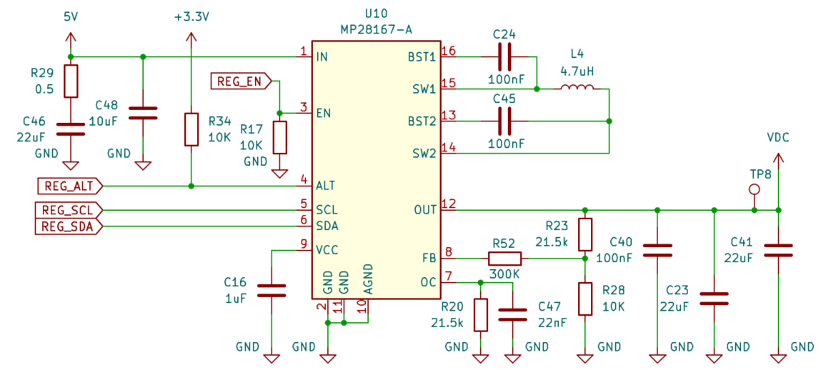
I really like the Nordic PPK2 for its software-adjustable output voltage and wanted to implement a similar feature for my project. The PPK2’s regulator works by combining an efficient buck-boost regulator with a low-noise LDO. Both are controlled by injecting analog control voltages into their feedback loops. While this works beautifully, the part count and overall complexity had me looking for easier solutions. This led me to the MPS MP28167-A, a buck-boost converter mainly designed for USB-PD applications. Instead of having to manipulate its reference voltage externally, it is fully controlled via I2C. The output voltage can be set in 0.8mV increments from around 1V to 5V, and even the current limit can be configured. Another great thing is that it decouples the voltage regulation completely from the Pico. Even a firmware reboot or crash won’t throw off the regulator’s voltage. It also only needs a few external components:
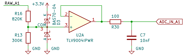
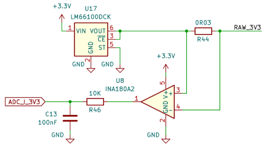 I added a basic analog front-end for the oscilloscope feature. It includes a high input impedance, an op-amp as a buffer amplifier, and an RC filter. This allows the RP2350 to sample voltages up to around 12V. In retrospect, a negative voltage range would have been a useful addition for measuring audio signals. I would definitely add this in a future revision of the PCB.
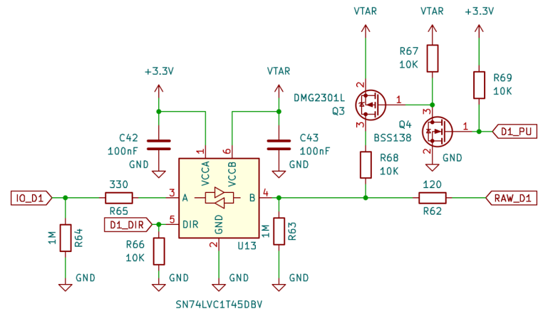
In addition to the 4 analog channels, the device has 8 digital GPIOs. These are used for the logic analyzer feature, as well as for directly controlling inputs and outputs. To make these GPIOs compatible with a range of target voltages, a level shifter is needed. I chose the SN74LVC1T45DBV because it has some nice protection features and is also used in the latest Bus Pirate boards. One side of this buffer is supplied by 3.3V, and the other by an external target voltage between 1.2V and 5V. One extra pin per buffer sets the direction (input/output). I also added a switchable pull-up resistor to each port. I was not sure if I could implement bus decoders in software, so I opted to include UART, SPI, and I2C on dedicated pins. They use the same circuit as the GPIO ports, but without the switchable pull-up and with fixed directions. Because I2C needs open-drain signals and I was too lazy to implement bit-banged I2C for the SN74 like the Bus Pirate does, I included a specialized level shifter: the PI4ULS5V202.
Discussions
Become a Hackaday.io Member
Create an account to leave a comment. Already have an account? Log In.