 Aleksei Tertychnyi


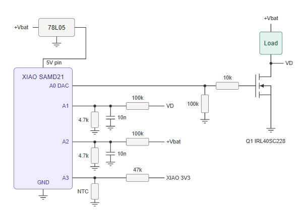
The load sits between +Vbat and the drain of an Infineon IRL40SC228, a 40 V logic-level N-channel MOSFET in D2PAK-7 with under 1 mΩ on-resistance. The source goes to ground. Since the MOSFET is in the load’s negative lead, the load voltage is simply:
V_load = V_bat − V_drain
Two resistor dividers (100 kΩ / 4.7 kΩ) bring the battery and drain voltages into the SAMD21’s ADC, which runs on its internal 1.0 V reference. At 20 V input the ADC sees about 0.9 V, giving roughly 5.4 mV of resolution at the input. A 10 nF capacitor on each ADC pin filters noise and gives the ADC’s sampling capacitor a charge reservoir.
The firmware runs a PI loop every 1.3 ms: average eight ADC samples per channel, compute the error against the setpoint, and update the DAC. The DAC feeds the gate through 10 kΩ, with a 100 kΩ pull-down on the DAC side of that resistor. Putting the pull-down there instead of at the gate means the gate sees the full 3.3 V (the gate draws no DC current), while still discharging through 110 kΩ if the DAC stops driving.
The interesting problems
The MOSFET is too good. A trench MOSFET with a huge die has enormous transconductance. Around its threshold voltage, a few millivolts on the gate change the current by amps. With a 10-bit DAC at about 3.2 mV per step, the loop works with only a handful of useful counts. The first, cautious tuning (slow integrator, 2 ms loop) made the load visibly blink, because the loop couldn’t follow load changes. Faster, stronger gains fixed it.
Loop timing hides in the ADC. In one version the loop period was set shorter than the time one pass actually took (24 ADC reads). The loop ran back-to-back, and the effective gain was set by the ADC speed rather than by the code. The current firmware measures its own worst-case pass time (dt_max) and counts overruns, so you can set the period honestly and know your gains mean what they say.
Integrator windup. When the battery is below the setpoint, the error stays positive forever and a naive integrator winds up to full scale. When the battery recovers, the MOSFET stays fully on until the integrator unwinds, which overshoots the load. The fix: if the drain is below 0.15 V, the MOSFET is already saturated, so stop integrating upward.
Serial interface
The XIAO’s USB serial port at 115200 baud accepts simple text commands:
V 13.2   → OK Vset=13.20
OFF      → OK OFF
P0       → OK P0      (stop periodic status, for scripts)
?        → status line + help
Every reply starts with OK or ERR, so it’s easy to script from Python with pyserial. The setpoint lives in RAM and resets to 12 V on power-up.
Protection
An optional NTC on the heatsink shuts the output down at 90 °C and restarts it at 75 °C. If the load voltage exceeds the setpoint by more than 1 V, the firmware pulls the gate down quickly. The XIAO itself runs from a 78L05 into its 5V pin, so the battery needs to stay above roughly 6.7 V.
Honest limitations
This is a linear regulator, so the MOSFET burns (V_bat − V_set) × I as heat: 24 W at 14.4 V in, 12 V out, and 10 A. Low setpoints at high current get extreme fast. The IRL40SC228 is optimized for switching, and trench MOSFETs can fail in linear mode well below their rated power, so check the DC line of the SOA graph or use a part rated for linear operation (Infineon Linear FET, Nexperia ASFET) if you push it.
Regulation also happens in firmware on a millisecond scale. Fast load steps will show short dips and overshoots. If you need fast transient response, put an op-amp in the loop and let the DAC set its reference. That’s the textbook solution, and the README covers it.