 Antti Lukats
This is the first lab setup I made. The R+C are on the backside of the blue proto PCB
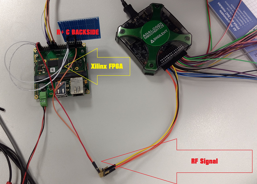
Yes the same setup was tested with 500Mhz signal as well..
A project log for 4R4C - FPGA Radio Challenge
We have 4 Resistors, 4 Capacitors and 1 FPGA to make RADIO Receiver.
This is the first lab setup I made. The R+C are on the backside of the blue proto PCB
Yes the same setup was tested with 500Mhz signal as well..
Discussions
Become a Hackaday.io Member
Create an account to leave a comment. Already have an account? Log In.
Please Do not "cringe" what ever it means, The two white wires are differential output from the mixer carrying signals in range of KHz only, this is not as nice as it could be, but for prototype testing OK. Analog discovery can only deliver max 10MHz, so the orange wire was used for 3.5MHz testing. The RF wiring is not visible at all, its on the backside of the PCB and done as RF as it can be done on perforated board. The "RF Input" is 2 pins 100 mil apart.
Are you sure? yes | no
I cringe when I see how you wire "RF signals" :-D
Are you sure? yes | no