YG asked for the schematic diagram of the balancer, so, I thought I post it here:
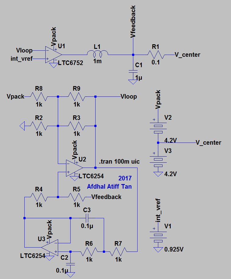
The circuit is the non-optimised version of the project. As you can see, the design is fully analogue with no expensive specialised chip.
I will update it to the optimised version at the end of the project.
The circuit should allow any buck converter chip to be controlled via a voltage reference (instead of a voltage divider network).
Feel free to tinker and contribute!
Discussions
Become a Hackaday.io Member
Create an account to leave a comment. Already have an account? Log In.
Interesting, thanks !
Are you sure? yes | no