Yann Guidon / YGDES
-
Assembler and disassembler
04/04/2017 at 23:42 • 0 commentsDevelopment with this kind of machine is "bare-metal". I'm simply tired of writing emulators and simulators, and people actually don't need much to get started : forget Eclipse or Emacs, just take some paper and pens. You can program a computer with something to input the instructions, and something else to read/decode the binary into human-readable form.
Following my experience with the #Discrete YASEP, I have decided to create a "hardware assembler/disassembler", using this kind of technology (sans the TTL ICs, see #Quick & Dirty Frequency Generator ):
![]()
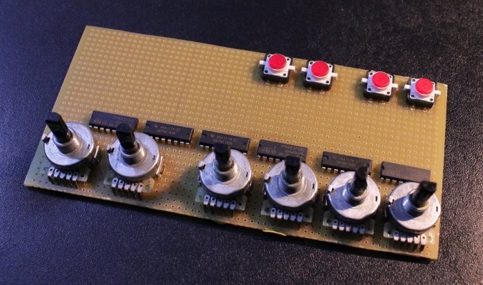
A set of two boards are connected to the instruction bus :
- The first board inputs data using knobs, in a manner that follows the instruction's logic and structure, and writes the corresponding bits on the bus.
- The second board reads the bus and displays the value, in a human-readable way (that is : with LEDs and maybe a #DYPLED)
If the user can take over the buses (instruction address bus, instruction read bus, ...), they can examine the program, input arbitrary instructions, single-step through routines, modify the memory and check the execution.
The assembler board provides one switch or rotating knob for each field :
- 4 knobs for the IMM16 field
- one for each source and destination register field
- one for the condition
- some switches and sliding switches to select modes and options
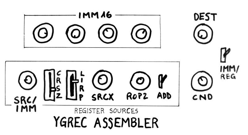
For example :
![]()
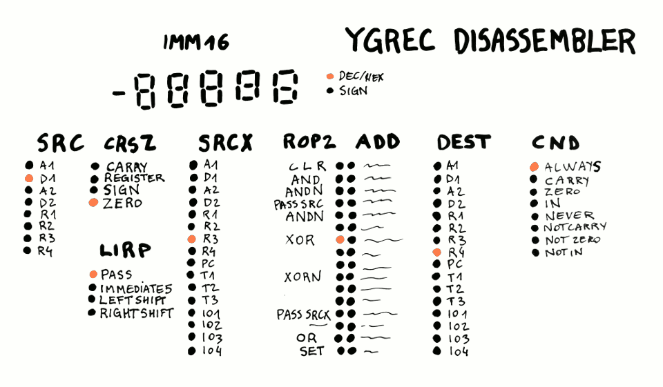
Note that the values of each position are not all marked because they are displayed in the disassembler board :
![]()
Little lamps show the value of the current instruction. In this example, we see the instruction "D1 XOR R3 => R4"
The disassembler board is always connected to the instruction read bus so you can see the machine's thoughts as it runs... But both the assembler and disassembler must be modular because they will be reused for the next implementations in various technologies :-)
-
PROM boards
04/04/2017 at 23:19 • 0 commentsNow that I know the instruction width, I can finally move forward with the design of the instruction memory.
The YGREC is a Harvard architecture and the instructions can be stored in read-only memory, made from diodes arrays.
There are programmable arrays, with switches that a user can change to affect the program. With 24-bits instructions, 3 standard 8-positions DIP switches fit nicely, but what about the physical dimensions ?
![]()
I've made a few attempts with the wrong switch model (still waiting for the definitive model) and the wrong kinds of boards but I have come to a few conclusions.
![]()
One Europe-format board can contain 16 instructions. I'll see if I can get cheap 20×16 boards etched for me.
The multiplexing is pretty important too but unlike the DRAM system, we're not forced to have a 2D array. I initially thought about adding relays on the result bus but I realise it's pointless : that's 24 relays... It's better to just select which board gets the address, and populate each instruction board with one relay per line.
At worst, the backplane can have 48 instruction bits, and select one half or another, to simplify the routing.
For the diodes : any kind is fine, I wonder if I can use bipolar transistors as well :-D After all a PNP transistor is a pair of common anode diodes, right ? Well, the base current might just kill the part... For now I must use the BAW56 (still waiting for them) and the trusted 1N4148.
For now I have determined the width of the boads : 16cm (enough to carry 48 data bits and address bits). A PROM board on a Europe card (10cm) will store 16 instructions, a double (20×16) contains 32.
Diodes-only boards can double this density but require more decoding.
The decoders are made of relays and we have seen that MUX require certain topologies to balance their fan-in. Modularity dictates the grouping of boards and 64 seems to be a good compromise. That implies 32 relays per group, which is a convenient and balanced configuration, see below, though reordering must be done, it might be advisable to make a separate board with one MUX32...
![]()
64 instructions is roughly the size of the core program that computes the #Game of Life bit-parallel algorithm :-)
Each board can be removed and possibly connected to other devices for programming : I'm thinking about building an electro-mechanical assembler/disassembler. A mechanical switch will select between the user input and the PROM board to ensure that the program is correctly configured (by comparing the disassembler's panel).
PS: Yes, I remember, there was the idea of using LEDs instead of diodes.
However the forward current and reverse voltages don't allow the use of standard LEDs... The RES15 require too much current to "trip" from one state to another (at least 40mA with pre-bias) and that might damage the LED if the current remains too long. Adding a parallel diode to limit the current would increase the cost further...
-
DRAM (again)
04/04/2017 at 21:17 • 0 commentsLet's start with the Program Memory. Or more exactly : the ROM.
It's made of a collection of diodes, making a diode matrix to store 24-bits words.
There is also the configurable ROM, which is made of boards with DIP switches.
For the ROM I can use my stock of leadless 1N4148 (SOD) and solder one diode where one bit must pass. But developing the software that must be soldered requires a development board, hence the DIP swiches, which is my focus now : 256 words require 768 DIPS switches (ok) and 6144 diodes.
Wouldn't it be nice if they were easier to solder ? The SOD diodes roll before soldering. OTOH I know there are dual-diodes in SOT23 : half the number of parts, 2/3 the number of pins to solder.
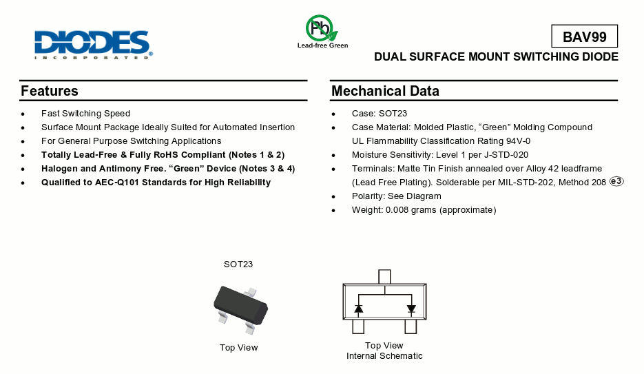
I use dual-diodes in the PWM generator of #DYPLED but I have the wrong kind, with no common anode or cathode. So I went shopping. And I found ... something else !
![]()
Further down the datasheet (well, the competitor's), I find that it's a "low leakage" diode. Low leakage, two diodes...
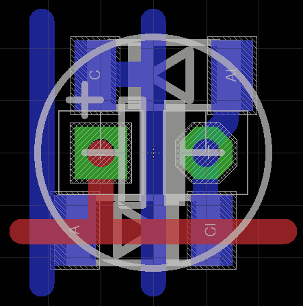
Yes, the DRAM cell needs that ! The SOD version was such a pain to route:
![]()
(see the log Dual Diodes (the hard way))
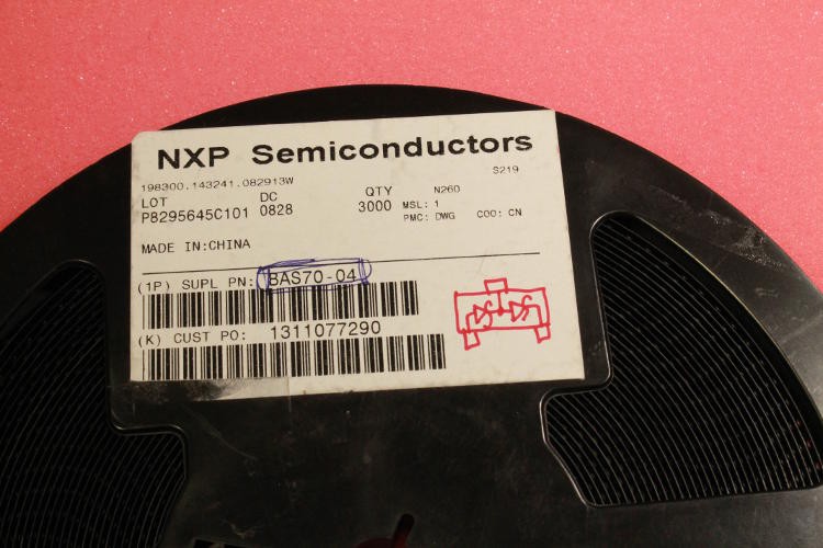
For now I can test a prototype array with the BAS70-04 (NXP) (I can borrow the reel from the #DYPLED project which doesn't need all of it) and I can compare the leakage, the driving methods, the routing...
![]()
Anyway I have vague estimates of the leakage currents, but no clear understanding of all the phenomenons at play in this kind of array. Fortunately the capacitors have a reasonably high capacitance and high voltage so maybe I can spy on the voltages with a 10x probe.
BTW a 512-words DRAM system requires 9216 dual-diodes... that's a lot and I plan on building 40 arrays of 16×16 bits (10240 diodes).
OK I made a little mistake : the BAS70 are very small signal Schottky diodes.
http://assets.nexperia.com/documents/data-sheet/BAS70_1PS7XSB70_SER.pdf
Schottky is usually more leaky than traditional 1N4148 (though it is relative to the voltage ratings). Their repetitive pulse ratings are also far from what the system will make them endure (12V differentials during contacts).
But it can be indicative of a "worst case" so why not try and measure the data retention time ?
PS
Happy ending : I have found some BAW56, with enough peak current rating, in SOT23, for the PROM array, but I must wait for their delivery... and only enough for 128 instruction.
-
Evolution of the architecture
04/04/2017 at 01:10 • 0 commentsWhat a day ! Where do I begin ?
Ah yes, yesterday, I was thinking about the I/O system.
With a budget around 500 relays, that translates to 50/18=27 relays per slice (I exaggerate because I/Os are not parity protected but "bear with me". That would be about 16 relays for outputs and 8 for input. BTW, what are these ?
- Input is simple : this is just an external signal that enters the datapath. One MUX per input channel is enough.
- Outputs are a bit more tricky : they need to be latched, so this uses two relays : one for selection and the other for storage.
Now, let's think about this:
- 8 read and 8 writes is ... very similar to the existing register set !
- It appears that 8×16bits of inputs AND outputs is quite a lot (128 inputs wires, 128 output wires...) and I don't think I can use all of them.
So today I merged the I/Os and the register set. This computer uses both "register-mapped memory" AND "register-mapped I/O"...
So far, we already have these 8 registers :
- A1
- D1
- A2
- D2
- R1
- R2
- R3
- R4
Fine, now let's add our four I/O registers:
- I1 / O1
- I2 / O2
- I3 / O3
- I4 / O4
(that's 64 input wires and 64 output wires, not bad...)
Reading I1 will read the corresponding pin while writing O1 at the same address will set the corresponding pin. They are only related by having the same address.
Now, what if you connected, say, I1 to O1 ? Well, you get a register (that can be seen by the exterior) and which can only be read by one MUX8.
And since we don't need as many GPIO, let's now introduce the "extended registers" ! Welcome to
- T1
- T2
- T3
The last one is, well.... hmmm I had to think hard about it but I have chosen to dedicate it to PC.
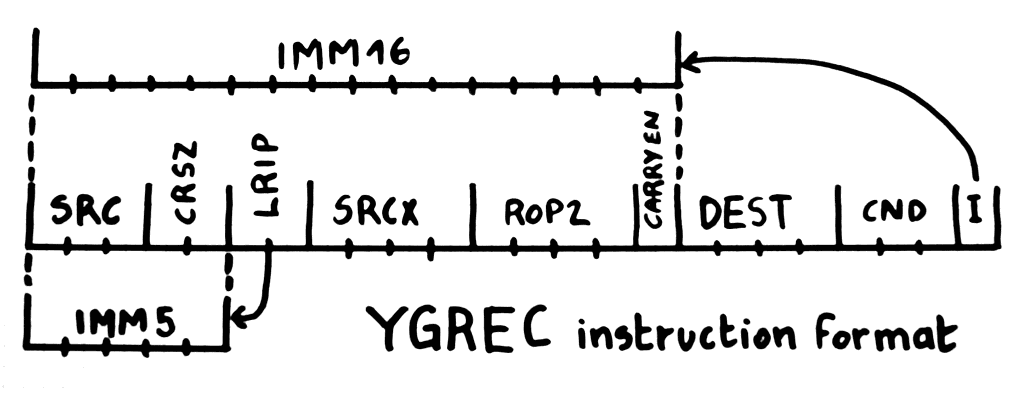
We have 16 registers, now, guys ! But one half can only be seen by the 2nd read port. The instructions contain these fields :
- SRC : 3 bits
- SRCX : 4 bits (SRC eXtended)
- DEST : 4 bits
SRC is missing some of the action but has its own fun : it gets the shifting done, and gets a bit of immediate values. Each slice can do :
- Pass (direct value from the register)
- Shiflt Left (1 bit)
- Shift Right (1 bit)
- Immediate (short)
(that's a MUX4)
The short immediate value comes from the SRC field, but 3 bits (range from -4 to +3) is a very short range. But there is more :-)
Usually, the complete set of operations is : ROR, ROL, SHL, SHR, SAR, and let's not forget the Carry : RCR, RCL, SHRC, SHLC, and the arithmetic SAR...
They only affect the "edges" of the shifter, so we have to select the value of the next bit that gets shifted in.
- 0 (for SHx)
- sign bit (for SAR)
- Carry (for SxC)
- the bit from the opposite bitplane (for ROx)
That's just a few relays on the edges of the backplane, that use 2 control bits.
We now have a more complete set of single-bit shift operations and 2 more bits to use with the short immediate, no dead code :-) The Pass function can also gain more features, I'll decide later.
(byte swap ?)
5 bits of signed immediate value is very short, and useful for short jumps for example, but the user needs to load whole 16-bits registers. There is not much room and I'd like to share features with the other instructions so I have decided :
- Common prefix : DEST (4 bits), Immediate flag (1) and CND (condition, a 3-bits predicate) [total: 8 bits, niiiice]
- The remaining 16 bits are either the immediate value or the source and ALU bits.
The source fields are :
- 0..2 : SRC (access the 8 lower registers)
- 3..4 : C/R/S/W (shift "edge" mode)
- 5..6 : R/L/I/P (Right, Left, Immediate, Pass)
- 7..10 : SRCX (access all the 16 registers)
Bits 11..15 are left for the ALU. 5 bits is just enough to do all the ROP2 and some funky add/sub dance.
Conclusion : the YGREC is a pretty complete computer now, with a 16-bits datapath, I/O and 24-bits fixed instructions !
The instruction format is very well adapted to the datapath and very little decoding/recoding is needed.
Two fields need to be defined : CND and ALU.
CND uses 3 bits : usually one if for the negation, two bits remain for the source :
- Always
- Carry
- Zero
- Input
The condition "not always" is "never", which is often an "extension code" , that I keep for later.
20170407: "never" is now the "call" prefix. Call can't be conditional/predicated but saves some efforts (at least one instruction) for routine management.
The "input" condition could be the value of one Input signal that is selected (MUX) by an output register. We will see...
There is something funky : the address registers are fully populated but only 8 or 9 bits are used. If you write values in the MSB, they will be ignored. This can be interesting for saving/hiding values... (It just needs a byteswap feature)
The PC however is external. Damn, I need to design an incrementer with CCPBRL...
The ALU Field uses 5 bits.
1 bit for the carry chain enable and 4 for the ROP2 MUX4.
When the carry enable bit is clear, the full standard ROP2 features are available : you write the LUT directly in the opcode.
When set, the ROP2 field is overwritten to XOR or XORN. One bit selects the Carry-in, another if the carry flag is written.
(to be determined later)
I love that the instructions are 24 bits wide, in particular because 3 8-positions DIP switches can encode one instruction. With the stock I have, I can wire about 256 instructions. This means that the PC needs to be 9 bits at most. OK let's say 10 but the system then needs to MUX on the backplane level....
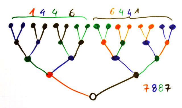
For the sake of completeness, the diagram that shows the instructions is here:
![]()
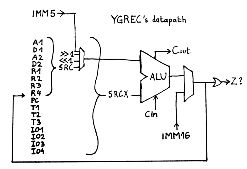
The overall datapath is now :
![]()
Even a kid could understand that, right ? :-)
I haven't included the rest, like DRAM, PROM, clock, tree drivers...
On 2nd thought : let's scrap the IMM16 MUX at the end of the ALU. Instead, send "Pass SRC" to the ROP2 and we're done. However the gain is not significant and probably negative because
- IMM5 is sign-extended but IMM16 is transmitted as is. That's 11 MUX2 to select the MSB.
- the ROP2/ALU control signals must be "overdriven" : that's 5 more MUX
No relay has been saved but it's more compatible with a transistorized implementation.
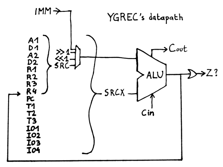
Here is the new version : it looks even more simple !
![]()
Of course it's simple because I have taken a lot out of the picture but this gives you a "programmer's view.
Update : I added the PC in the datapath in 7. The Program Counter's circuit