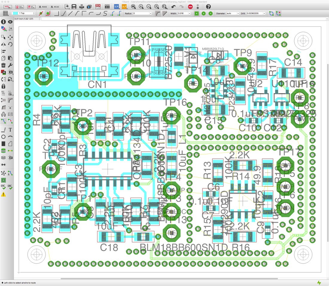
I have been learning EAGLE layout. My review so far is "Good, not bad. Could be better."

I like the interactive routing, and the MOVE command works well for moving existing routing. Not all tools are good at this. I need to learn more to do a real comparison. After using PCB layout for about 12 hours, I think I am better at it than I was after using gEDA/PCB for 12 hours. I am much better than I was with much more expensive CAD tools after 12 hours. I haven't tried KiCAD for that long, so I have no comparison for it.
There are some things that bother me about it: The polygons are painted, and not very well. This means that sharp-cornered polygons don't seem to be possible. After a while of using gEDA/PDB, I got to the point where I could make it do anything that I wanted. With EAGLE, I have to make the usual tradeoff: I can't draw exactly what I want, but what I can draw is more productive.
There has been one crash, but I lost very little work by manually renaming an auto-saved file. It did not offer to restore this file for me. The program briefly flashed an error message about some missing object as it went down during an UNDO. After launching it again, it didn't offer me an auto-saved file, and it had been 30 minutes since my last SAVE. Weird. I found the tip that the autosave files exist from Google search results. Google results are one of the best parts about EAGLE. There is a lot written about it online. EAGLE has more good advice online than the Open Source tools I have used. It also has much more online than the 100X and 1000X more expensive tools. If you are using the Guess-Google-Guess-Google... learning cycle, it works fine.
There are some delightful things about EAGLE layout. One is the icons. The downside of my 4k monitor is that many applications have tiny icons and no way to make them larger. Some applications let you scale the Icons. The EAGLE 2X icons have high resolution, and they are just the right size on my 4k display. They are crisp! This is a true retina application. Nice! This is my first PC layout design with a 4k monitor. There is no way I am going back, because 4k layout is amazing. Applications without scaling capability have fallen behind where they need to be.
In the example screenshot, there is a lot of label clutter because I have the component values turned on. It looks better with just reference designators and net names. The net names help. For this type of layout, I am not just making connections. Layout is an important part of the design, and I have to understand exactly what I am hooking up, and how. There is cross-highlighting to the schematic to help with this. Also, I have named all the nets, and now I am getting the payoff for this extra work.
The proof of the CAD tool is in the Gerber output. I won't really know what I have until I look at the design in an independent tool.
 Tom Anderson
Discussions
Become a Hackaday.io Member
Create an account to leave a comment. Already have an account? Log In.