 Miroslav Zuzelka
So Revision B,
this is exactly same design as Revison A, just with fixed mistakes.
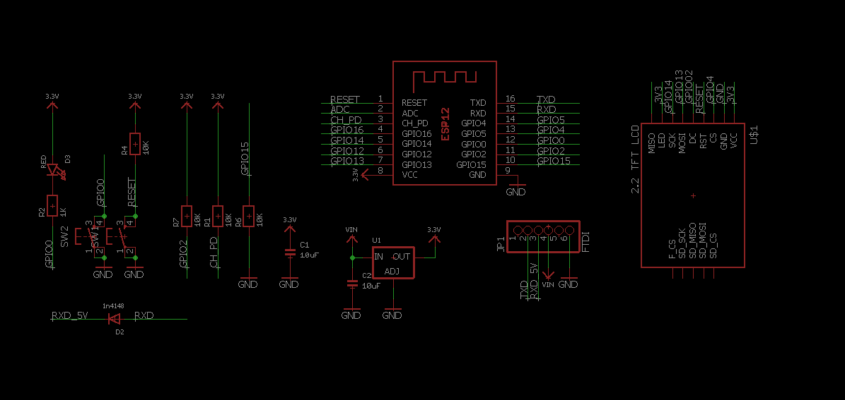
Schematic is same:
Board design looks like this:
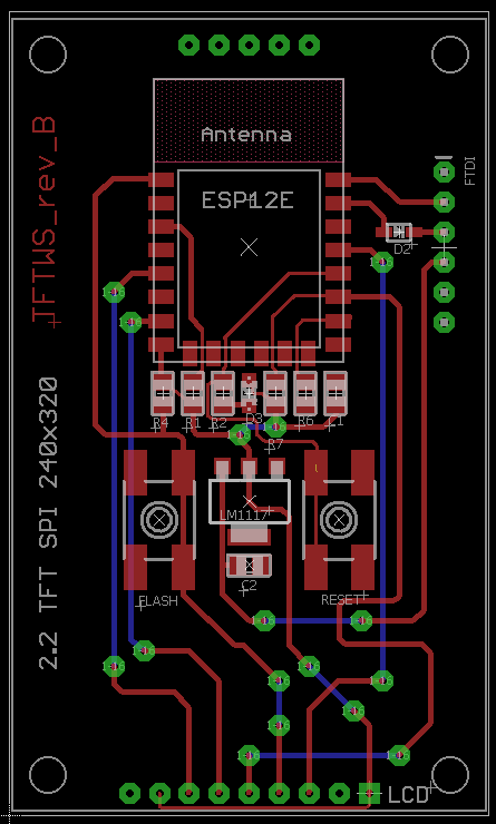
I rearranged parts so board looks more symetric and I changed buttons for bigger one.
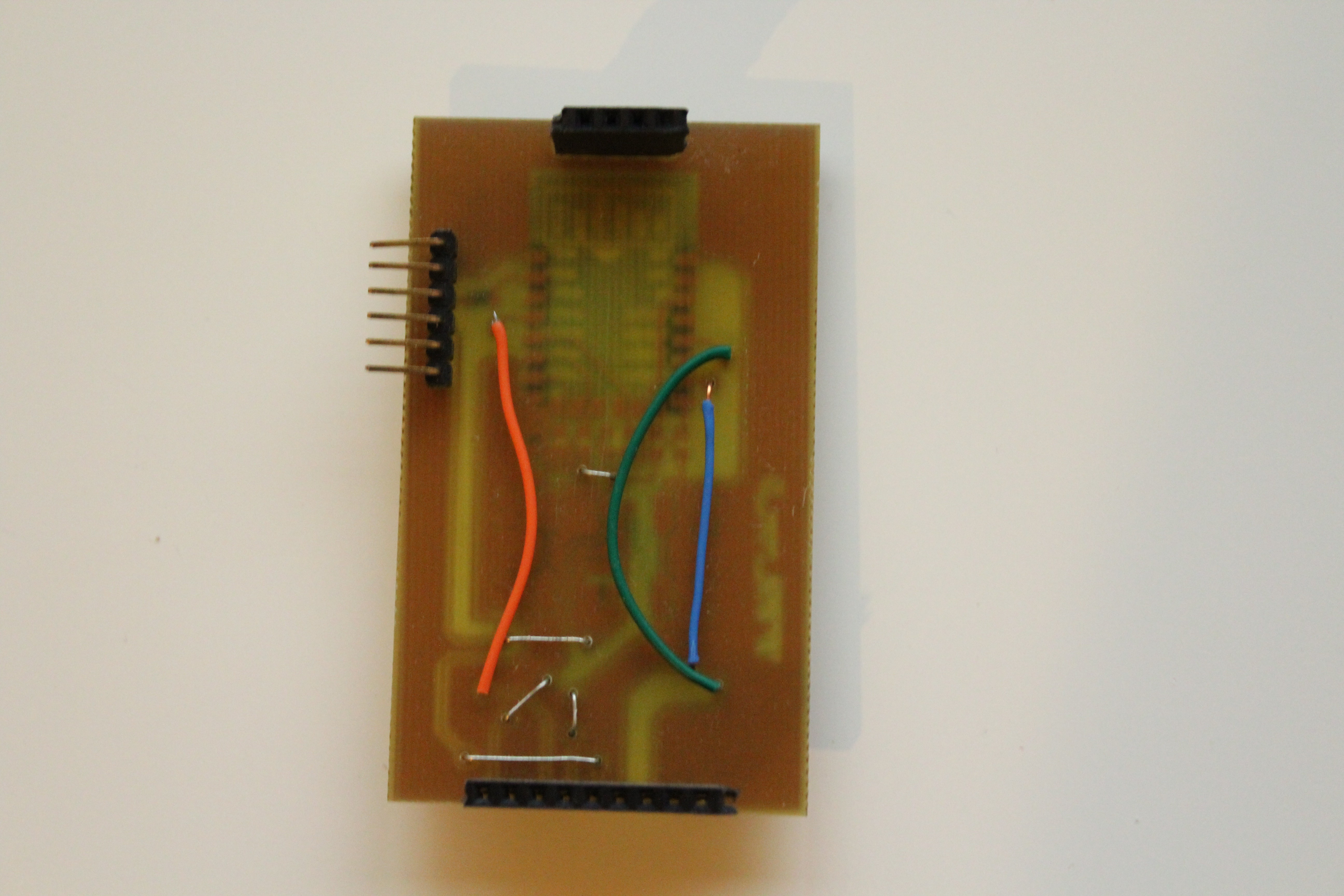
If you wondering why are vias so big, that is beacause if I will make them small, they will be hard to solder or they will fall of the board. Because my friend don´t make vias like normal PCB factory, I must have this in mind when I design my boards. It´s not big problem for me, but you have to think about it when you make your design. Again I have no picture of the board when I picked it up so here is board how look like now:
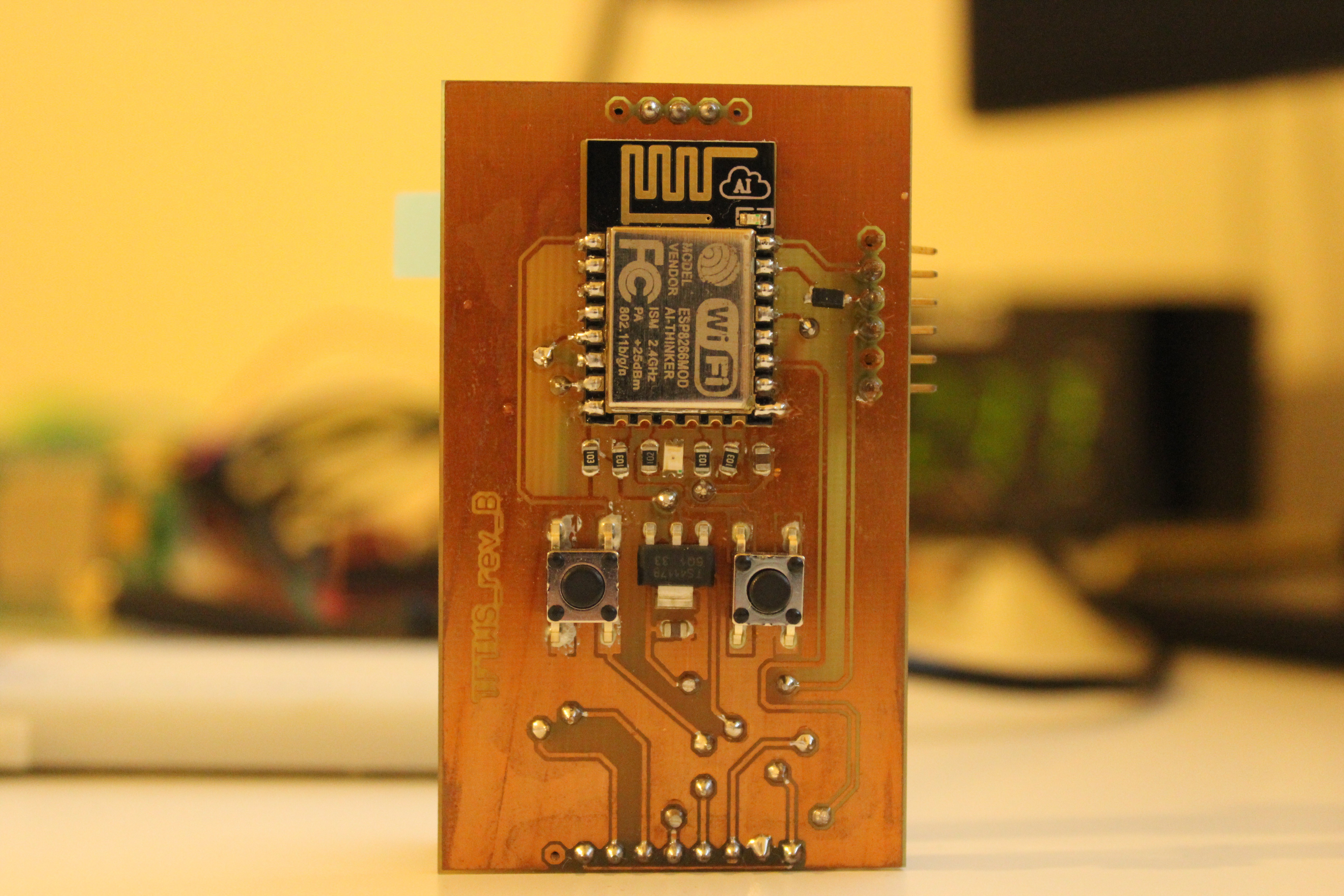
I had no problem with this revision = I don´t have to fix something :-p ;-).
Are you asking how do I flash it? It is same procedure like with any EPS without auto-reset feature: when you are holding flash button, you press reset button and it will jump in the programming mode and you can cklick Upload button in your Arduino IDE ;-).
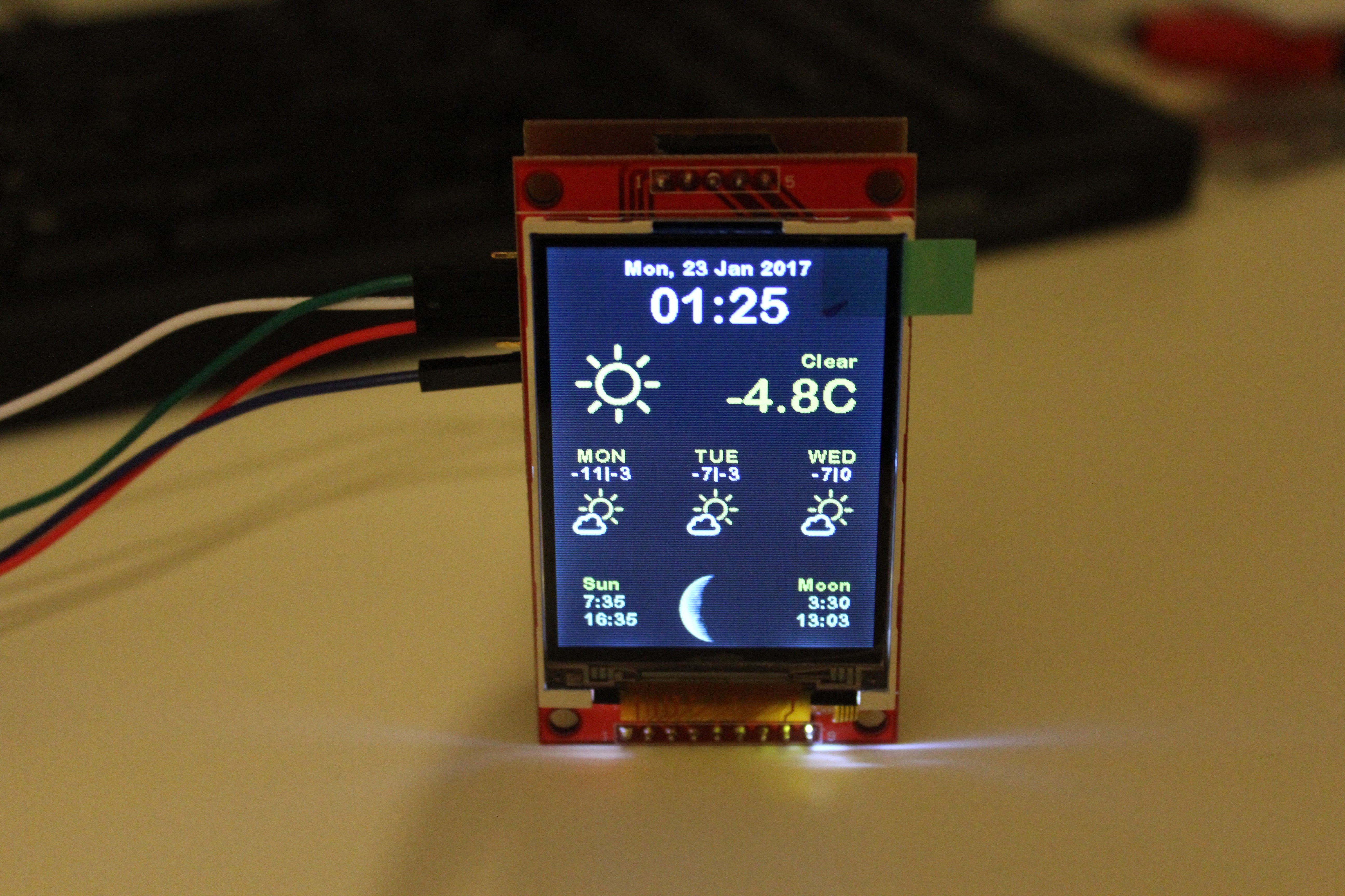
Here is result of that procedure:
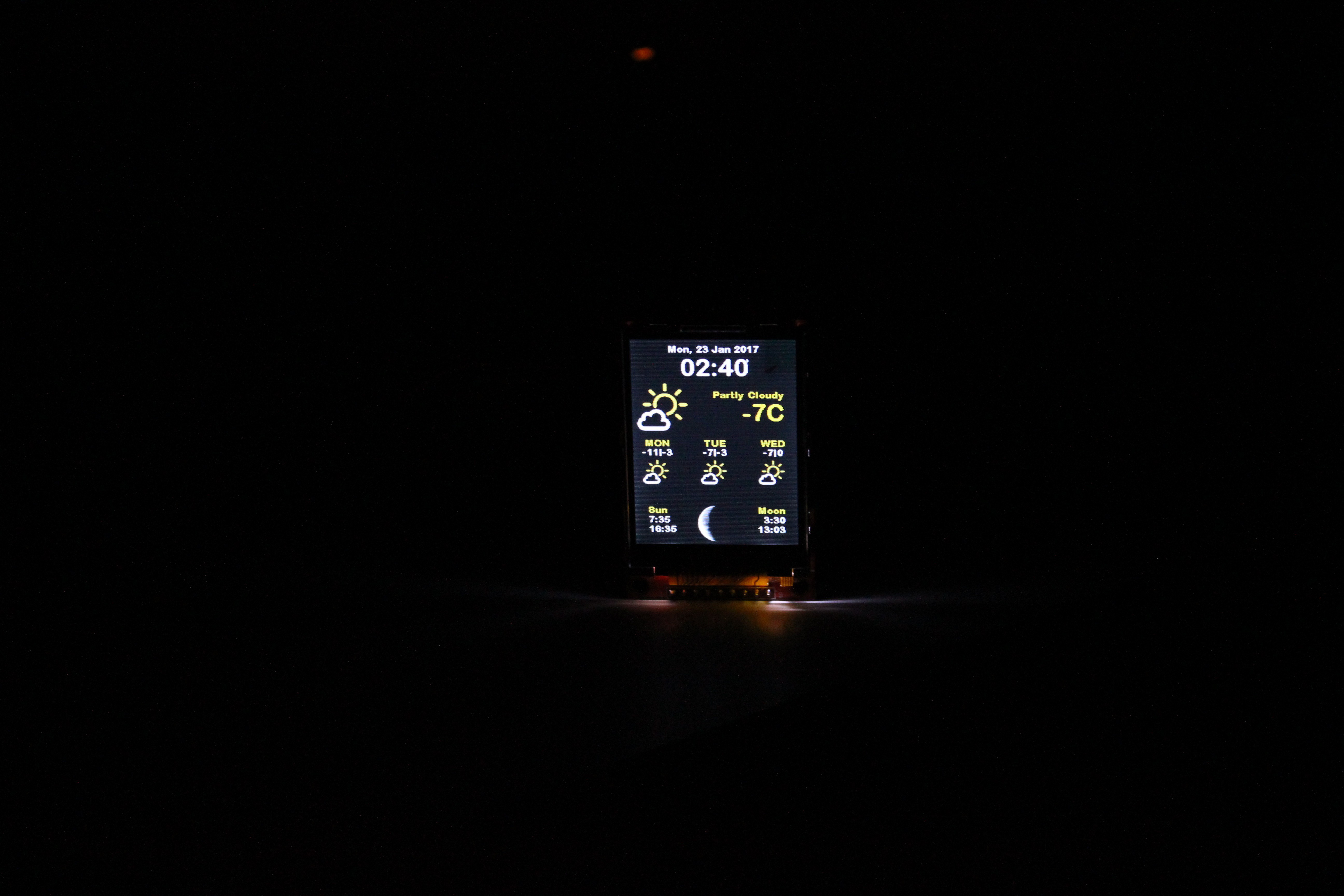
Here is how it looks like in the dark:
That´s all for this revision, if you have any question, let me know in discussion ;-).
See you soon with another revision.
Discussions
Become a Hackaday.io Member
Create an account to leave a comment. Already have an account? Log In.