 Bruce Land
-- VGA display using a bus_master as a GPU for the HPS. Display from SDRAM.
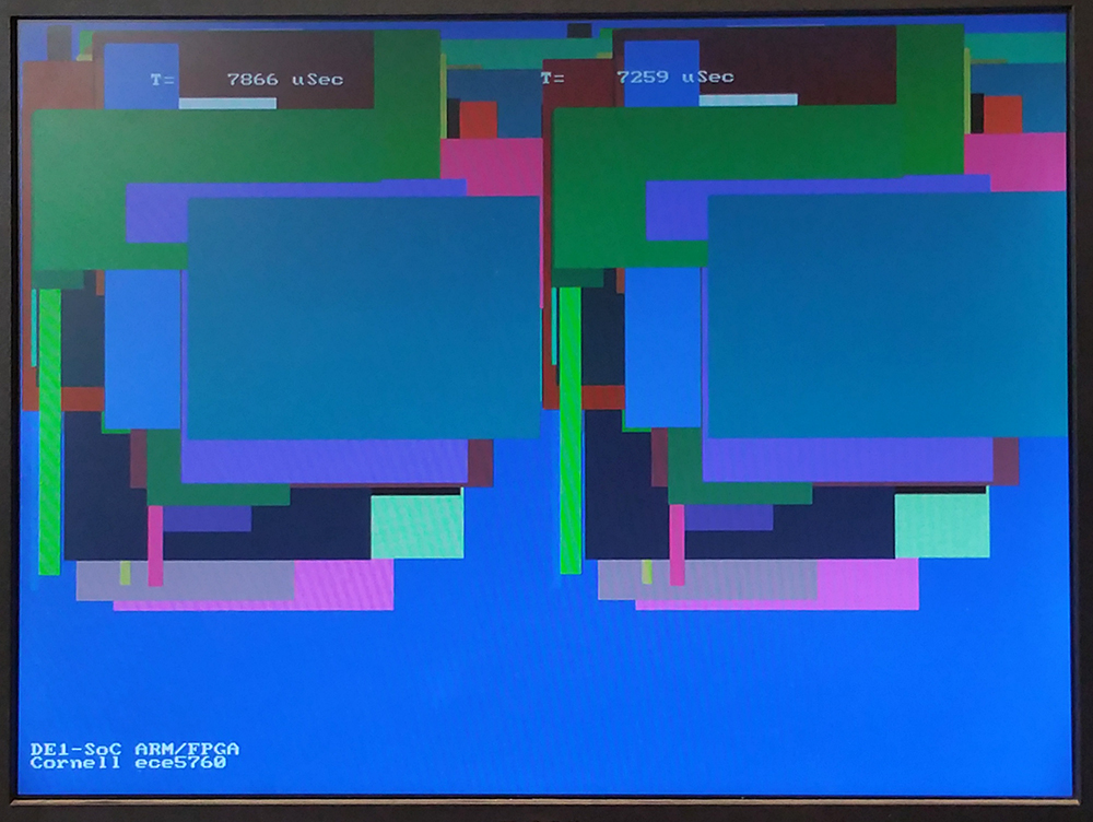
A simple GPU was written that only writes rectangles. It takes corners
(x1,y1 and x2,y2) and colors from the HPS in SRAM scratchpad memory and
displays them into SDRAM-buffered VGA. The SDRAM is therefore shared
between the HPS, the GPU bus_master, and the VGA controller in Qsys. The
SRAM scratchpad is shared between the HPS and the GPU bus_master. The
HPS is attached to SRAM scratchpad using Qsys, but the bus_master is
attached in the FPGA fabric, not in Qsys. The bus_master state machine
reads five values from the scratchpad, then drops into a loop until both
x,y exceed their limits. The loops includes a write operation to the
bus (4 cycles), plus a delay to allow the VGA controller to access
SDRAM. With a 50 MHz state clock, eight wait states are required in the
delay to avoid video artifacts. The number of wait-states can be set
using the upper four switches from 0 to 15. This results in about 4
pixels/microsceond write rate, about the same as the HPS. The first HPS
code queries the command line for five numbers, where x1<x2,
y1<y2, and color 0-255, then draws on the left side in hardware and
on the right side from the HPS. The second HPS code draws rectangles as
fast as possible to test for stability. Again, the left and right sides
of the screen are written respectively from hardware and from the HPS, and should match (HPS code1, HPS code2, top-level, ZIP)
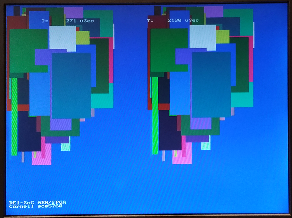
-- GPU with FAST display from SRAM.
The write rate of the above SDRAM-buffered VGA is low, so I rewrote the system to use dual-port SRAM for the VGA buffer.
One port (s2) is connected through Qsys to the VGA controller and HPS,
as usual. The other port (s1) is exported to the FPGA fabric, and
connected directly to the GPU state machine in Verilog. The clock bridge shown
syncs the the SRAM slave port to the GPU state machine. The logic to
control the GPU state machine from the HPS is unchanged from above.
Direct connection of display memory to the GPU state machine results in a
write-rate of 48 pixels/microsecond. To get the high rate, the GPU
state machine was rewritten to pipeline writes to the VGA display SRAM.
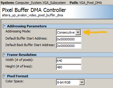
To minimize on-chip memory use, the display mode was changed from x/y to
sequential, saving 30% of SRAM. To make the mode change, the VGA_pixel_DMA module dialog box in the VGA subsystem needs to be modified. The HPS code is also changed to reflect the modified display mode. The left and right sides of the screen
are written respectively from hardware and from the HPS, and should
match. The times at the top of the screen are the writing times for
hardware and software respectively. (HPS code, top-level, ZIP).