 JohSchneider
the pcb is straight forward
- smd diodes: according to their markings, bottom side
- io-expander: only one per pcb, bottom or top
- switches: in triplets, aligned with the help of a small jig
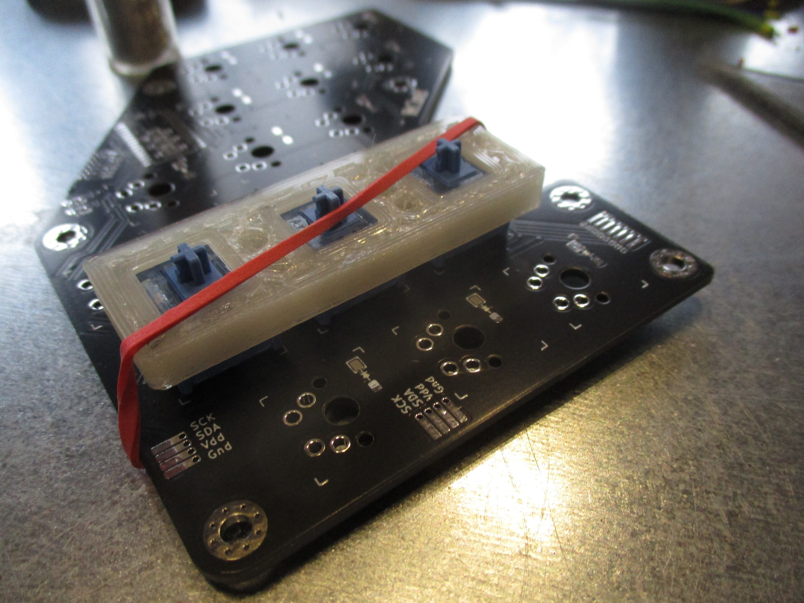
the thumbcluster is a little more effort :-)
1. the printed part has M3 screw holes, which need to be tapped
2. each switch is prepared with a THT diode
3. each switch gets it's own "column" wire, threaded through the PCB slot
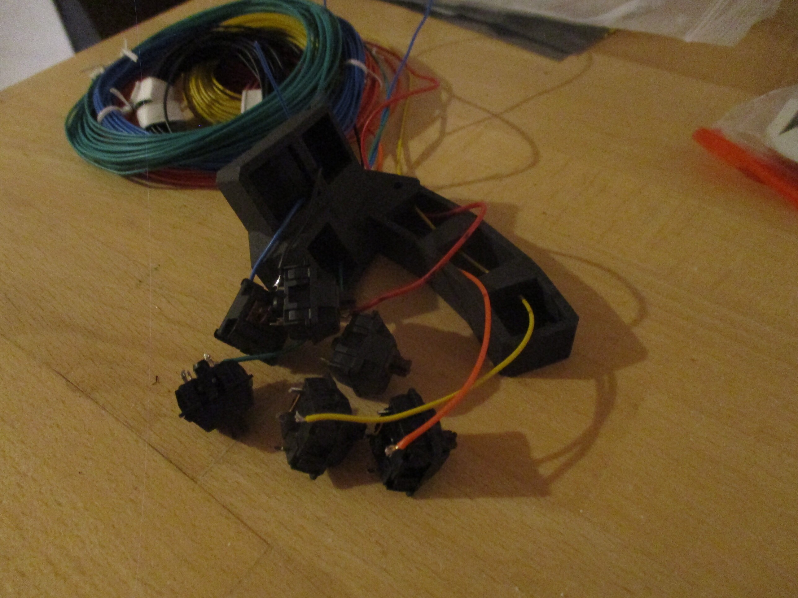
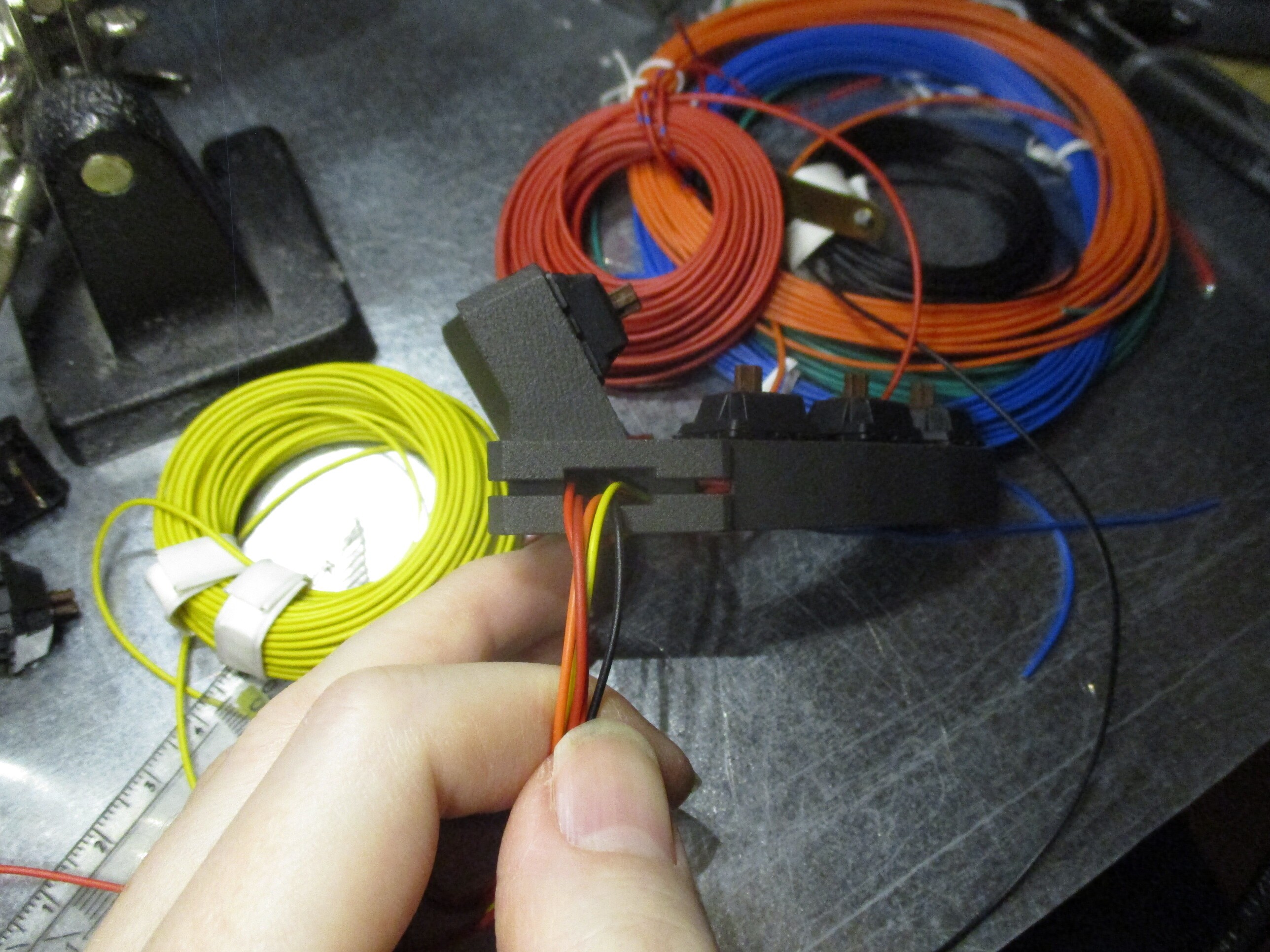
4. the "row" wire is prepared: 4cm+4cm+6cm+4cm+4cm+spool
5. threaded through and soldered to the switches
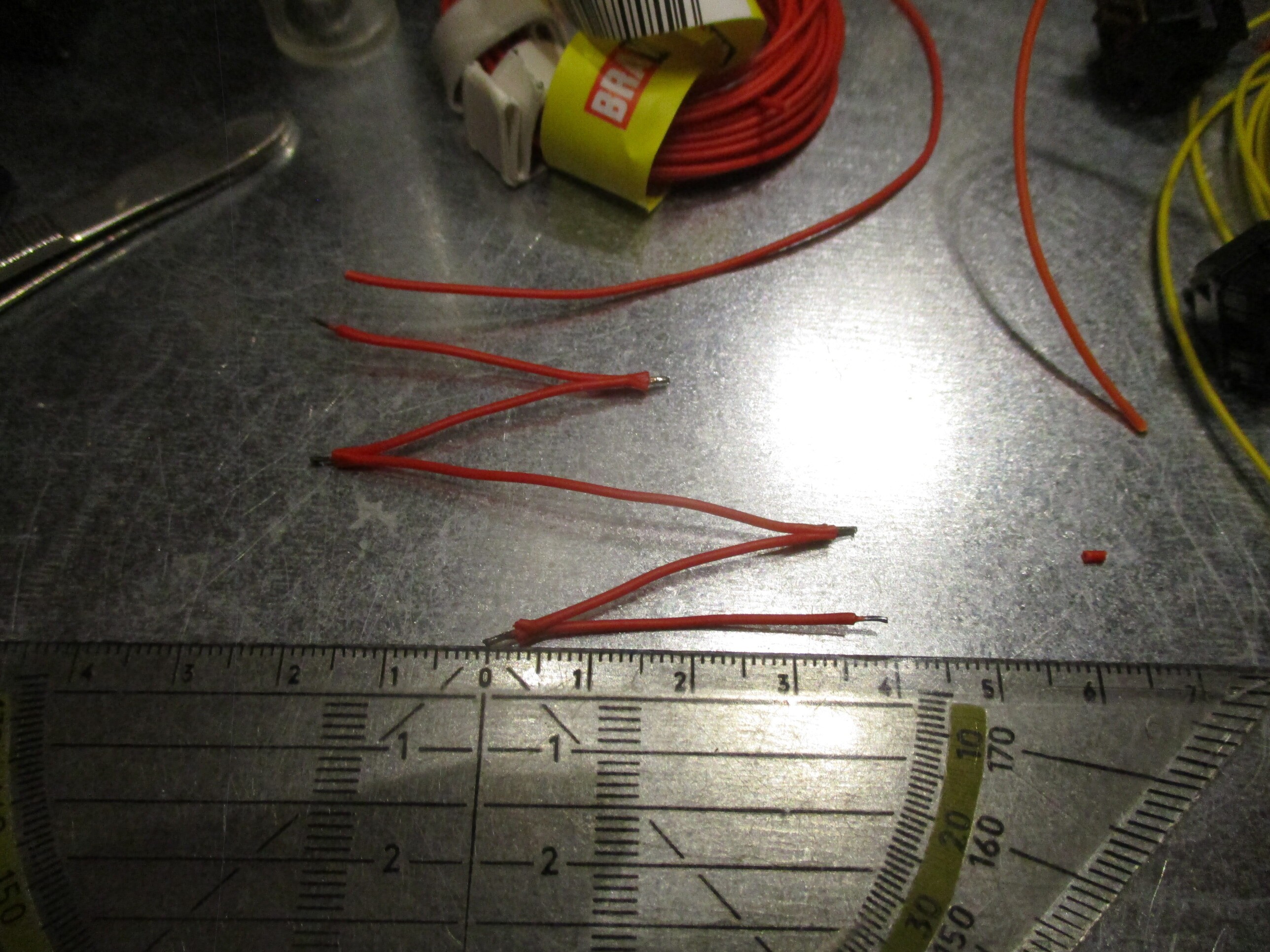
6. the wires are cut to length, checked that they run all through the central hole (and not any small adjacent ones) and stripped
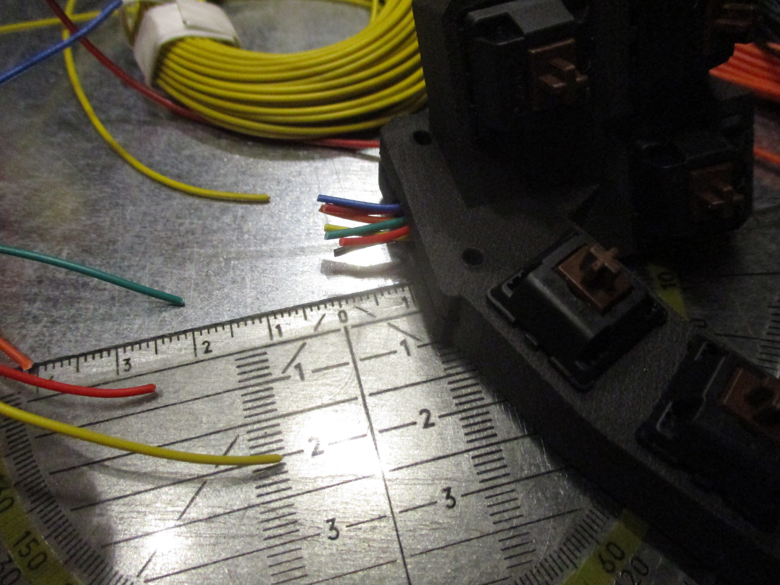
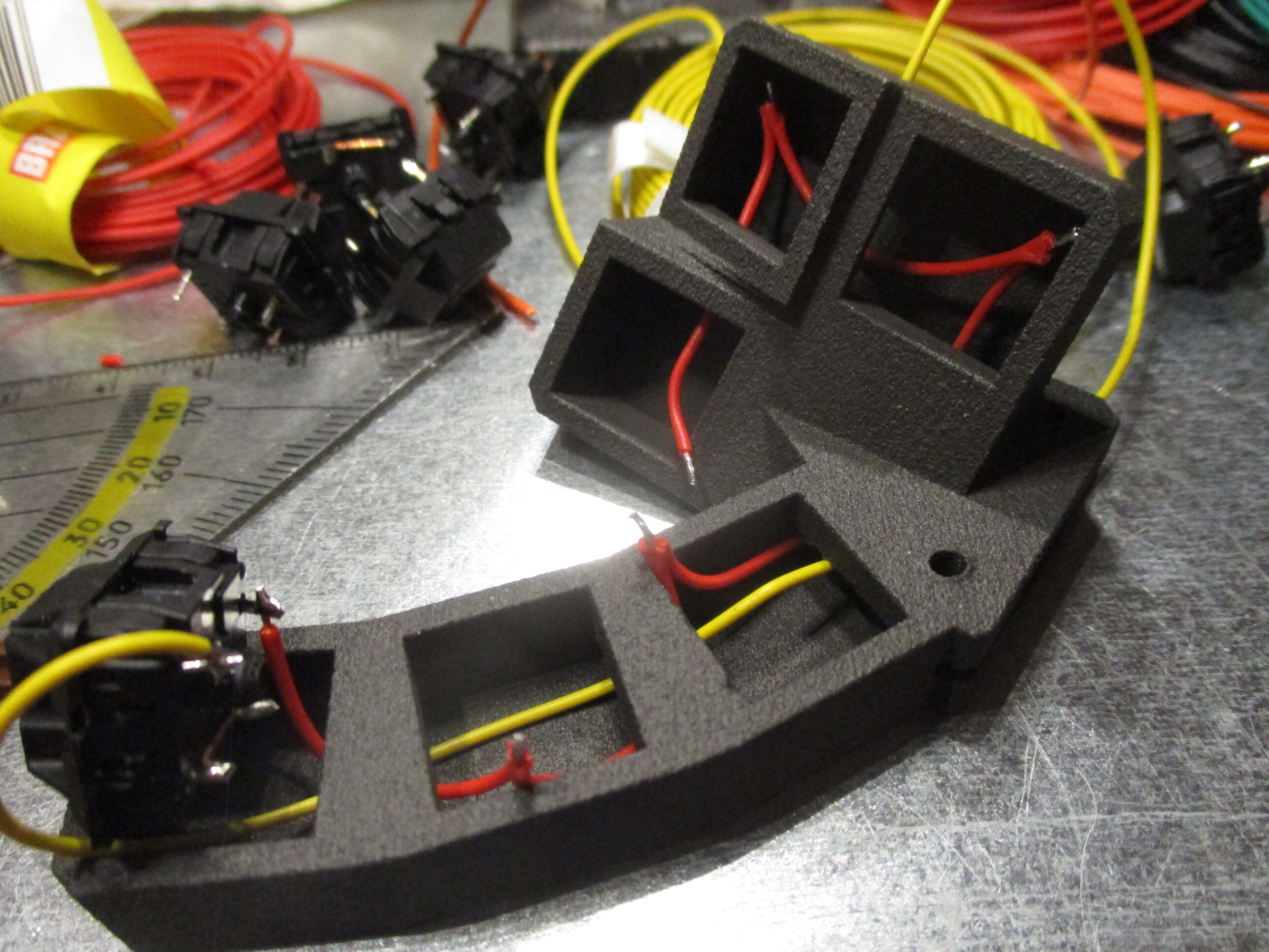
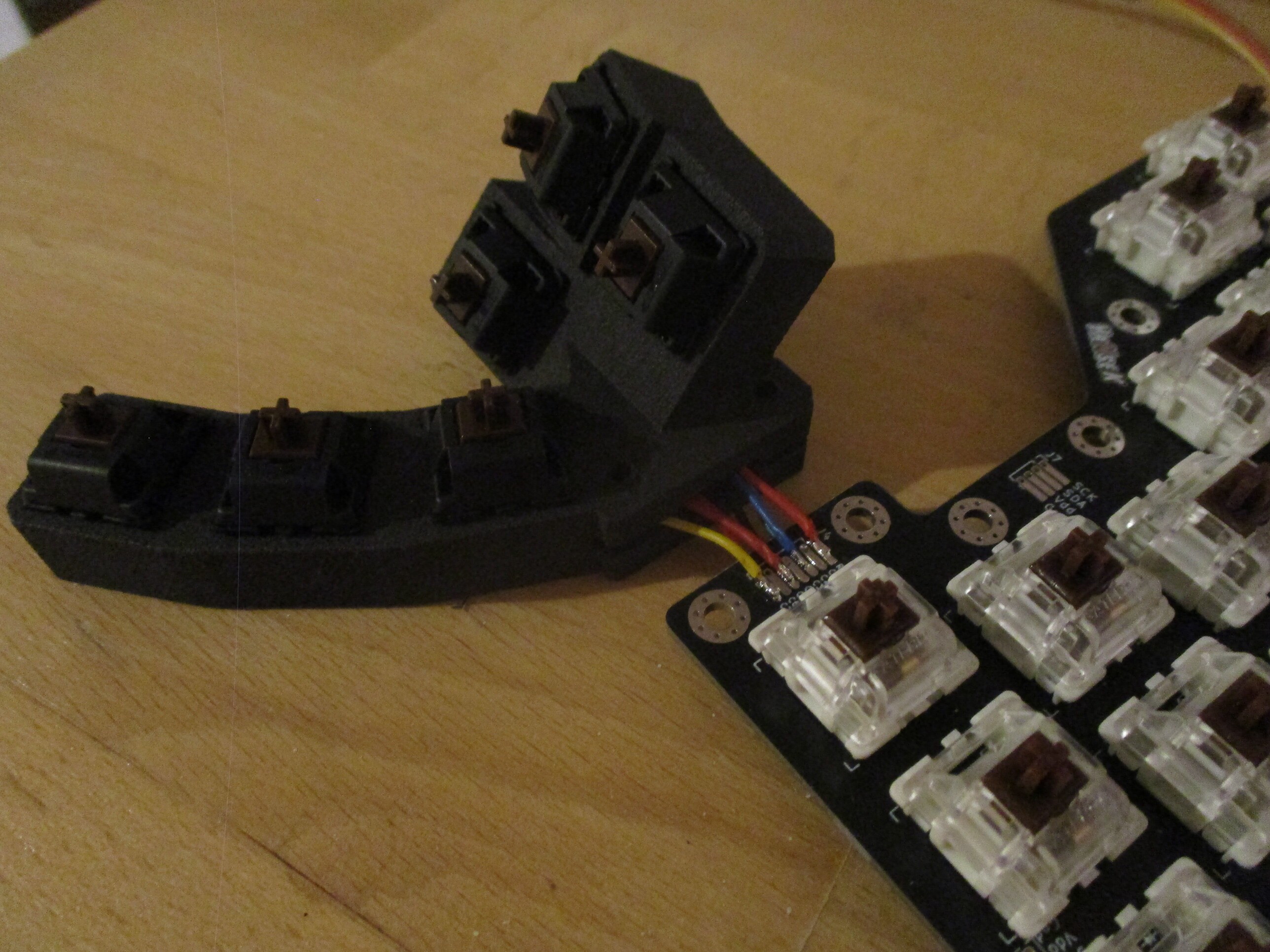
7. connecting to the pcb:
since the pads are available on both sides, and spaced for a ribbon cable, alternating between front and back
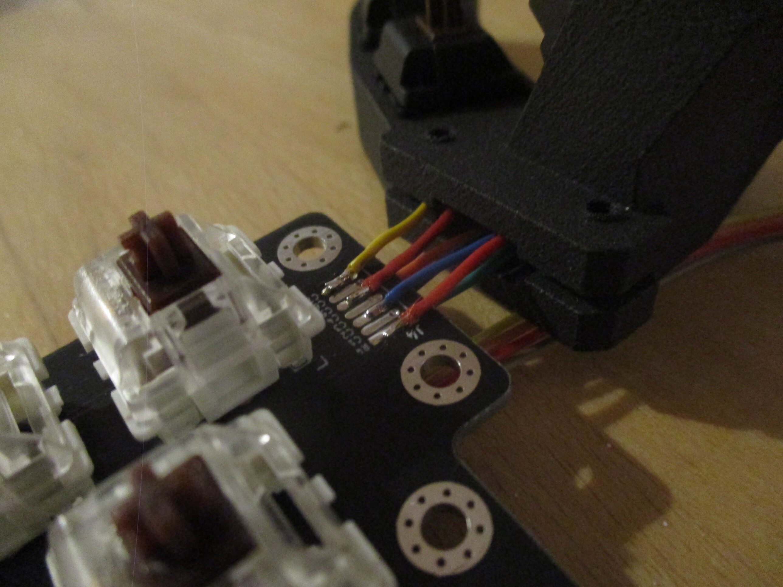
Note on the column order, and color coding:
chose *the same* color codes for the left and right assembly. since the pcb is flipped, so is the order
e.g. the left side has from left to right C0...C5; where as the right side has from left to right C5...C0
in the above picture, the leftmost key has a yellow wired, connects to C5 pad - and would do the exact same for the right side
Discussions
Become a Hackaday.io Member
Create an account to leave a comment. Already have an account? Log In.