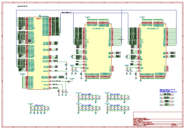
After I split the repositories into sub modules I started shuffling things around in the schematics. There is not very much done, but the switch to i.MX7 CPU is coming along. I copied the PMIC and DDR design from my test project and merged it into the current design. Next big thing will be mass storage and multimedia. I want to keep up the current design where I can switch between mic as input for the GSM module on the one hand and CPU as source on the other.
I played around a little bit with the Android build system. It is big. I think I need to go a little bit deeper into it to finally wrap my head around it. Anyone there who has experience with building Android?
This is the RAM schematic so far. Data signals will be assigned when it is tie to route the bus to the chips.

 Platinenmacher
Discussions
Become a Hackaday.io Member
Create an account to leave a comment. Already have an account? Log In.