First and foremost, this is my first PCB so please be indulgent.
This being said:
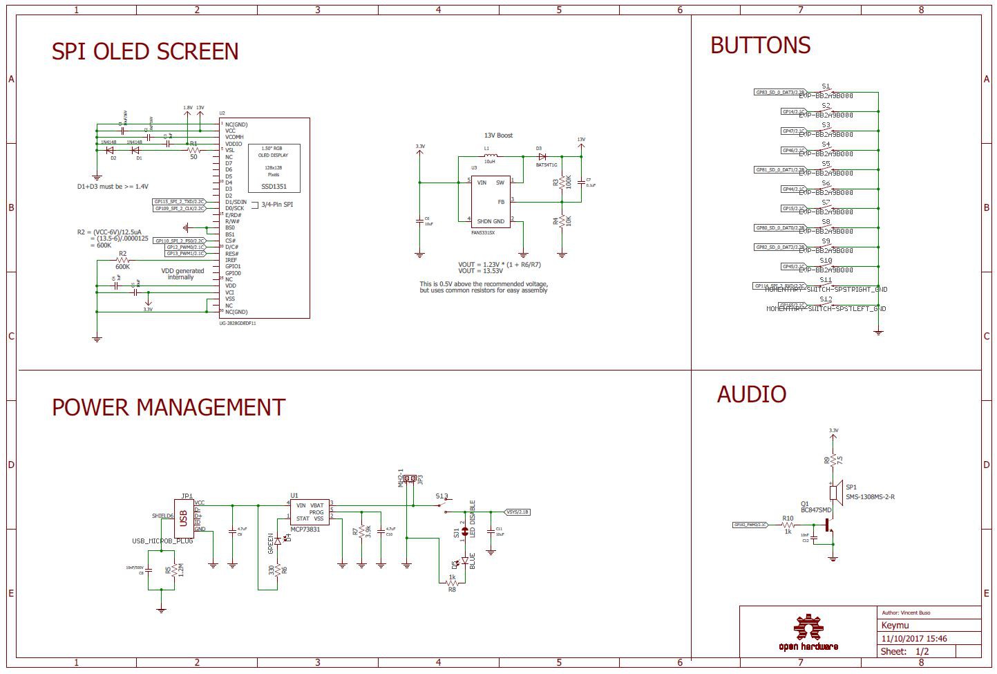
- You can download the schematics in the project files or here.
- You can download the BOM in the project files or here.
I prefer writing a log about this instead of build instructions, since this is more of a discussion of the schematics/BOM than proper build instructions. Of course, any comments/critics are very welcome so that Keymu can benefit from everyone's knowledge.
Schematic
Keymu was built around five mains blocks visible on the schematics:
- page 1 : Power management, screen management, buttons, and audio
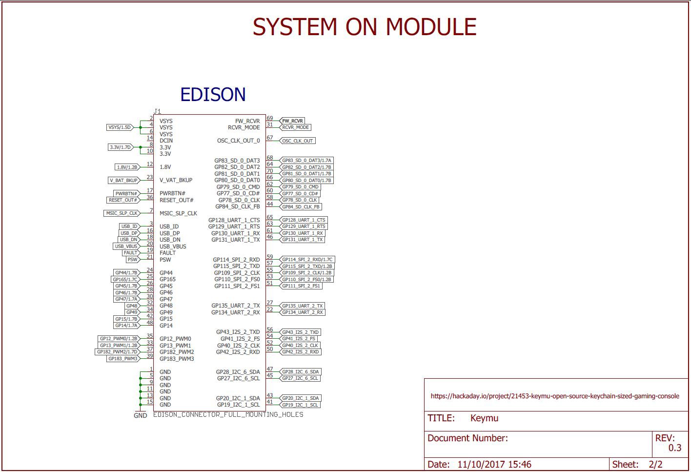
- page 2: The Edison itself
Power management:
This block was mainly inspired from Sparkfun's Battery block for the Edison.
Basically there is a MCP73831 linear charge management IC which does all the job of charging the battery from the micro-usb port. There is also a power switch to turn on/off the supply of current to the rest of the system (while still allowing the battery to charge), a blue LED to indicate if the system is turned on and a green LED that lights up when the battery is fully charged.
The few changes from sparkfun's battery block are :
- RC circuit with high supported voltage connected between the micro-USB shield and the ground to handle electrostatic charges,
- Changed R7 resistor value to charge 220mAh batteries at 1C.
Screen block
This block is almost fully based on adafruit's 1.5'' OLED Breakout Board. The only difference here is the VDDIO input signal of the screen which is set to 1.8V (instead of 3.3V) which is the Edison's GPIO's working voltage. The screen is also powered by the 13V boost converted and communicate with the edison through SPI.
Audio Block
Even though the last version of Keymu does not output audio, it is not the hardware's fault but the developer's one (guilty). The hardware is all there, and now Keymu needs the corresponding Kernel drivers to drive it. There is no DAC on the Edison so the chosen solution was to drive the speaker through a transistor delivering 3.3V with a PWM signal. Even though the sound quality is not the greatest, this is a well known solution and costs way less space (and price) than driving an external DAC with I2S. There is a great article about PWM audio in Make magazine, and this is the solution used for the Edidoom project as well, where it can be seen that the sound quality is not that bad, especially keeping in mind that the final product is a keychain.
PushButtons
Not much to say about this part, this is pretty much simply a matter of connecting the switches to the edison's GPIO's on one side and ground on the other. This is possible since we use the internal pull-ups of the edison allowing to save space and an easier rooting.
Board layout
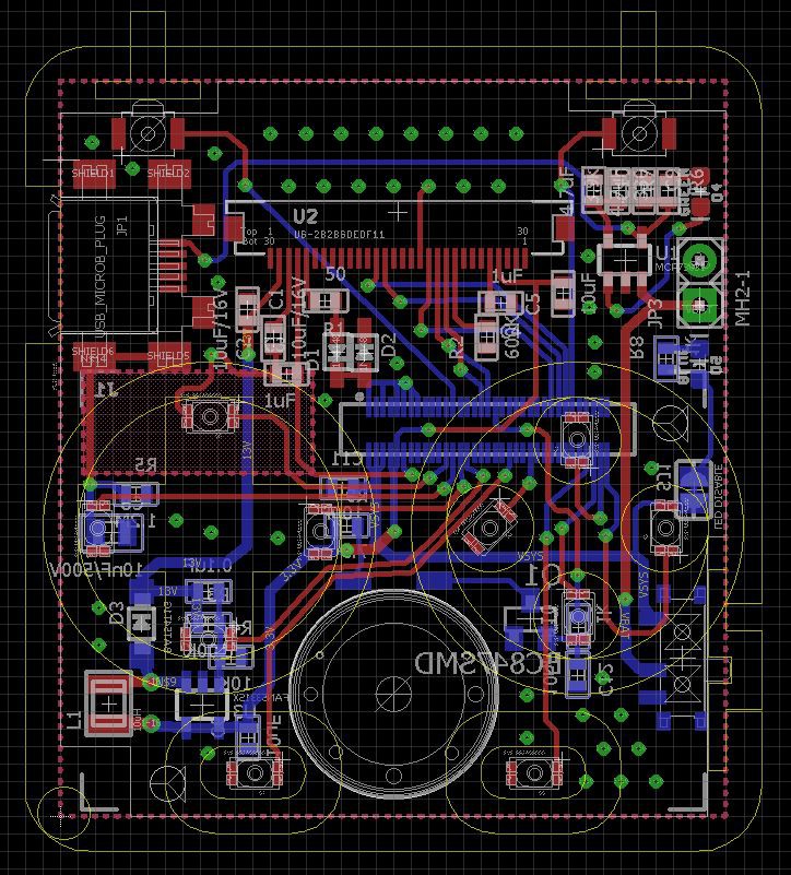
The full board layout can be seen on the following snapshot:
This is a bit of a mess to untangle so I will be discussing the top and bottom parts separately in the following paragraph. One thing to notice though is the yellow superposed drawings of the mechanical design for the casing and the buttons.
Top side
For more clarity here is the top part of the PCB:
It can be divided into two main parts: the higher one and the lower one. The lower one is mainly dedicated to the pushbuttons. It is quite had to find some space for other components in this part because otherwise it could prevent the full course of the mechanical parts above the pushbuttons.
The higher part is dedicated to the microUSB on the left, the screen connector and dedicated components in the middle, and power management with battery connector on the right.
Bottom side
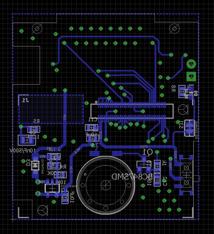
and here is the bottom side:
Here again it is divided in two: this time the lower part contains the Edison connector and all the components under the Edison: 13V DCDC boost convertor on the left, audio block on the right of the speaker and the on/off switch on the right. The top part is totally free of componnents on purpose: this is where the battery is located.
I know the writings on the board are pretty unreadable, my apologies in advance.
Printing the PCB
If you want to print this PCB, I sincerely recommend OSH park but there are many other options. This is free publicity for them since I was very happy with their service. I chose the 1.6mm depth for the PCB since it was a bit faster to arrive, but if you want to make Keymu easily slimmer, you can also choose the 0.8mm option. Here is what the PCB looks like:

Ordering the components...
From what can be seen in the BOM I tried to get most of the components from the same place, which is to say in this case: Mouser. The reason for Mouser over Digikey is mostly because shipping costs are free after 50$, but most of the components are standard and can be ordered from basically any main reseller.
The cost of components to build one Keymu is around 112$ (95€) counting the PCB from OSH Park, but not counting various shipping costs for components not available on Mouser and not counting also the 3D printed enclosure.
I would say the final price (counting everything) is around 150$, but of course it's an approximation. If you start ordering the same component in large quantities for exemple, the price decreases a lot. One exception though is our dear Edison chip which is damn expensive regardless of your efforts.
All things considered, prototyping Keymu is quite expensive, and that is why we are working hard on greatly reducing the price for the next iteration.
...and soldering it all together
Whoah, you're here. Great so it means you are ready to get your hands dirty.
I have to be frank this part is long, fastidious and requires some pretty high end material, but if you are here already, then listen to our old pal Nike and just do it (dammit).
First do not make the rookie mistake I made and hope you can soldier everything with your bare eyes and with a 50$ soldering iron from Amazon, just don't. Some of the components parts are very small like the pins of the edison connector, and some other are not only small but very sensible to heat like the pushbuttons. In ordier to soldier Keymu, a binocular is highly recommended, and you'll also need a high quality soldering iron. I used the professional material we have at work and it still took me around 2 hours to soldier both sides. If there is a hackerspace close to your place, I recommend going there and using their material for this kind of soldering.
Another rookie mistake, for those who might not know or the clumsy like me: it goes without saying but diodes have only one working side, careful to soldier them in the right direction.
What else to say? Good luck, just put some of your favorite music in your ears and it's actually quite a good head clearing time.
 c.Invent


Discussions
Become a Hackaday.io Member
Create an account to leave a comment. Already have an account? Log In.