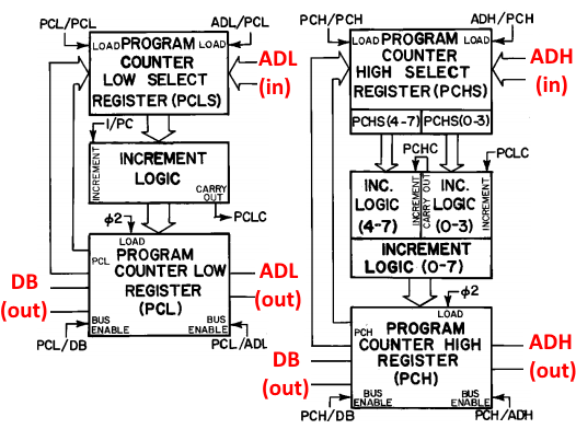
Next up, we’ve got the 6502 program counter! The PC is going to keep track of where we are in the program at any given time. Because the 6502 has a 16-bit address space, the PC has 2 8-bit registers for the low and high byte, respectively (it has 2 separate registers instead of 1 16-bit register, because some of the addressing modes handle the low byte separately - we'll get into this later). The operation of the PC is fairly straightforward, it gets loaded with a particular value, and then will increment that value as the program progresses (controlled by the cycle/opcode decoder mentioned last time). I’ve added the block diagram below to show the registers and inputs/outputs:
 It looks a bit complicated, because (a) you have to have
some logic to increment the high byte when the low byte overflows, and (b)
there are a couple of input/output choices to load and shuttle the PC around as needed.
For (b), you can load the PC with either the current PC value (to simply
increment to the next byte), or with the contents of the address buses (low
byte, high byte, or both). If you’re wondering what the deal is with the
high-byte incrementer being split into bits 0-3 and 4-7, you’re not alone. I
still am not sure what that’s for… anybody got some clarification? Ah well, we’ll
just ignore it for now. Here’s some code!
module ProgramCounter(
	input wire sys_clock, rst,         // Main system clock and reset
        input wire clk_ph2,                // Phase 2 clock enable
	input wire [7:0] ADLin, ADHin,	   // Address Bus low & high bytes
	input wire INC_en, 		   // Increment PC enable
	input wire PCLin_en, PCHin_en,	   // Use current PC
	input wire ADLin_en, ADHin_en,	   // Load new value into PC
	output wire [7:0] PCLout, PCHout   // PC Bus output
    );


// Declare signals:
reg [7:0] PCL, PCH;		// PC register low & high bytes
reg [7:0] PCLS, PCHS;		// PC select register low & high bytes
reg PCLC;			// PC low-byte carry bit (to increment high-byte)
reg [7:0] PCL_inc, PCH_inc;	// Incremented PC

// Select PC source: previous PC or new value from Address Bus:
always @(*) begin

	if (PCLin_en)
		PCLS <= PCL;		// load previous PC register value
	else if (ADLin_en)
		PCLS <= ADLin;		// load address bus value
	else
		PCLS <= PCL;		// default: previous PC

	if (PCHin_en)
		PCHS <= PCH;		// load previous PC register value
	else if (ADHin_en)
		PCHS <= ADHin;		// load address bus value
	else
		PCHS <= PCH;		// default: previous PC

end

// Increment PC:
always @(*) begin

	{PCLC, PCL_inc} = PCLS + 1'd1;	// Increment low-byte with carry out
	PCH_inc = PCHS + PCLC;		// Increment high-byte with carry from PCL

end

// Latch PC on phase 2 clock:
always @(posedge sys_clock) begin

	if (rst == 0) begin		// initialize PC to zero (will be replaced)
		PCL <= 0;
		PCH <= 0;
	end
	else if (clk_ph2) begin
		if (INC_en) begin	// if Increment enabled, latch incremented PC
			PCL <= PCL_inc;
			PCH <= PCH_inc;
		end
		else begin		// else, latch passed-through value
			PCL <= PCLS;
			PCH <= PCHS;
		end
	end

end

// Assign outputs:
assign PCLout = PCL;
assign PCHout = PCH;


endmodule
Ok, pretty straightforward here too. I’ve included the address bus as an input so we can grab the value as needed. I’m just including a single output for the current value of the PC, and we’ll let the instantiating module deal with shuttling it to where it needs to go. The module will select the input to the incrementer as either the current PC or the address bus, then will go ahead and produce an incremented value based on that (leaving the original unincremented, since we don’t know for sure whether we’ll be instructed to increment or not). Then, on phase 2 of the cycle, we’ll latch either the incremented or original value into the PC register for output.
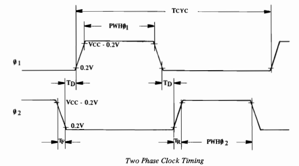
Hmmm, I guess I should talk about clocks… Right! So, first, all synchronous logic in the NES implementation runs off a single system clock to avoid timing issues (note that the ALU last time was purely combinational, with no clocks). Second, the 6502 actually does a funky thing with its clock: it splits every clock cycle into 2 phases (see the overcomplicated timing diagram below):

So the input clock to the 6502 is inverted to form the phase 1 clock (phi_1 in the diagram), which is then inverted again to form the phase 2 clock (phi_2 in the diagram). Each CPU cycle contains both a phase 1 and a phase 2 clock. All timing in the processor is specified based on one of those two phases. For example, in the PC diagram above, the PCL and PCH registers get latched on the phase 2 clock (see the little phi_2 symbol on the "load" input). We’ll get into this more later, but basically, address output are latched on phase 1 and data is read or write from memory on phase 2. Make sense? Cool.
I think that’s it for the program counter, next up: the instruction controller (not the decoder just yet, just the hardware for loading in an opcode).
Discussions
Become a Hackaday.io Member
Create an account to leave a comment. Already have an account? Log In.