 Hexastorm
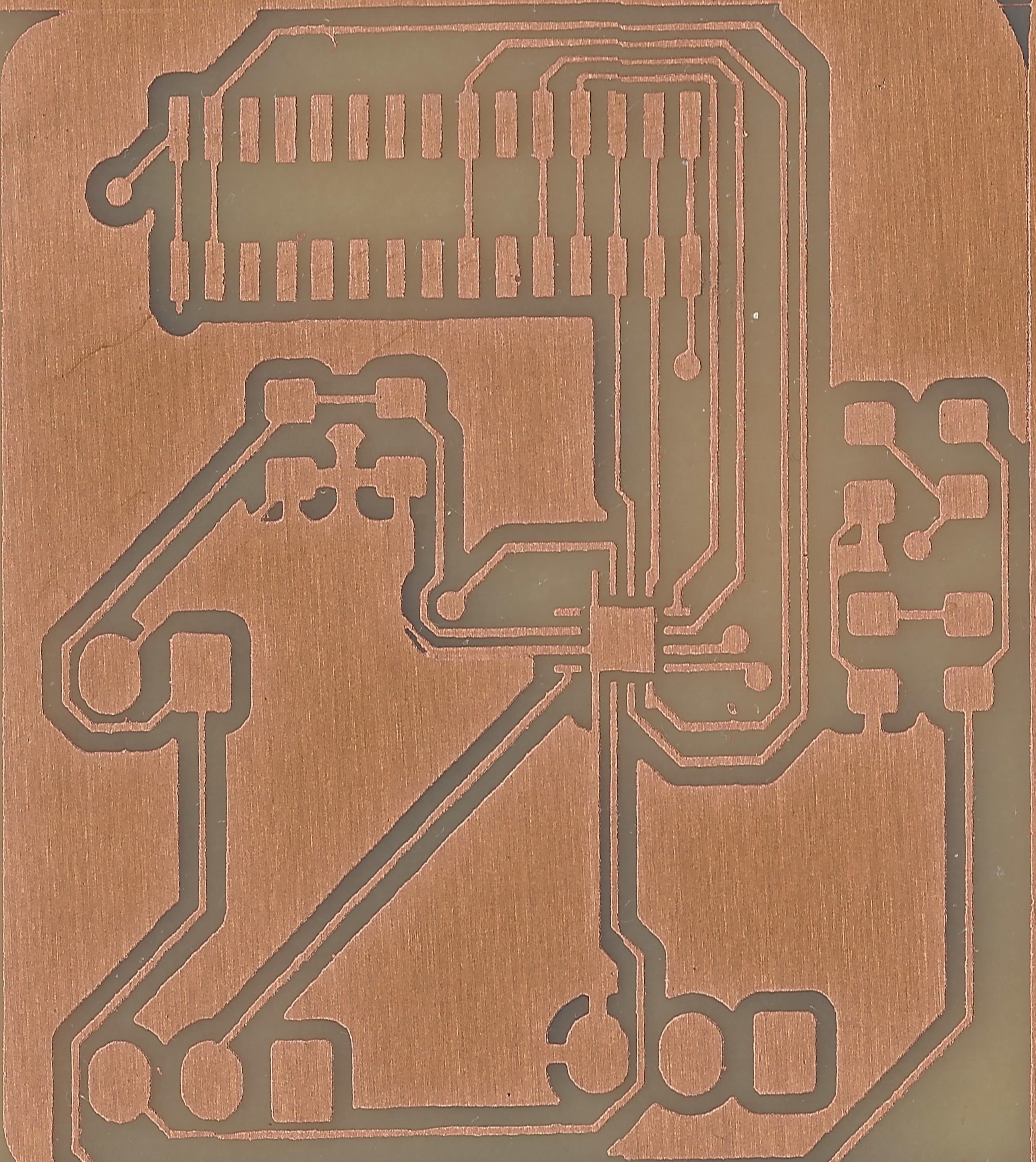
I succeeded in making some PCbs using laser direct imaging and prisms.
Track width of board below is 250 microns... the bronze colour is copper
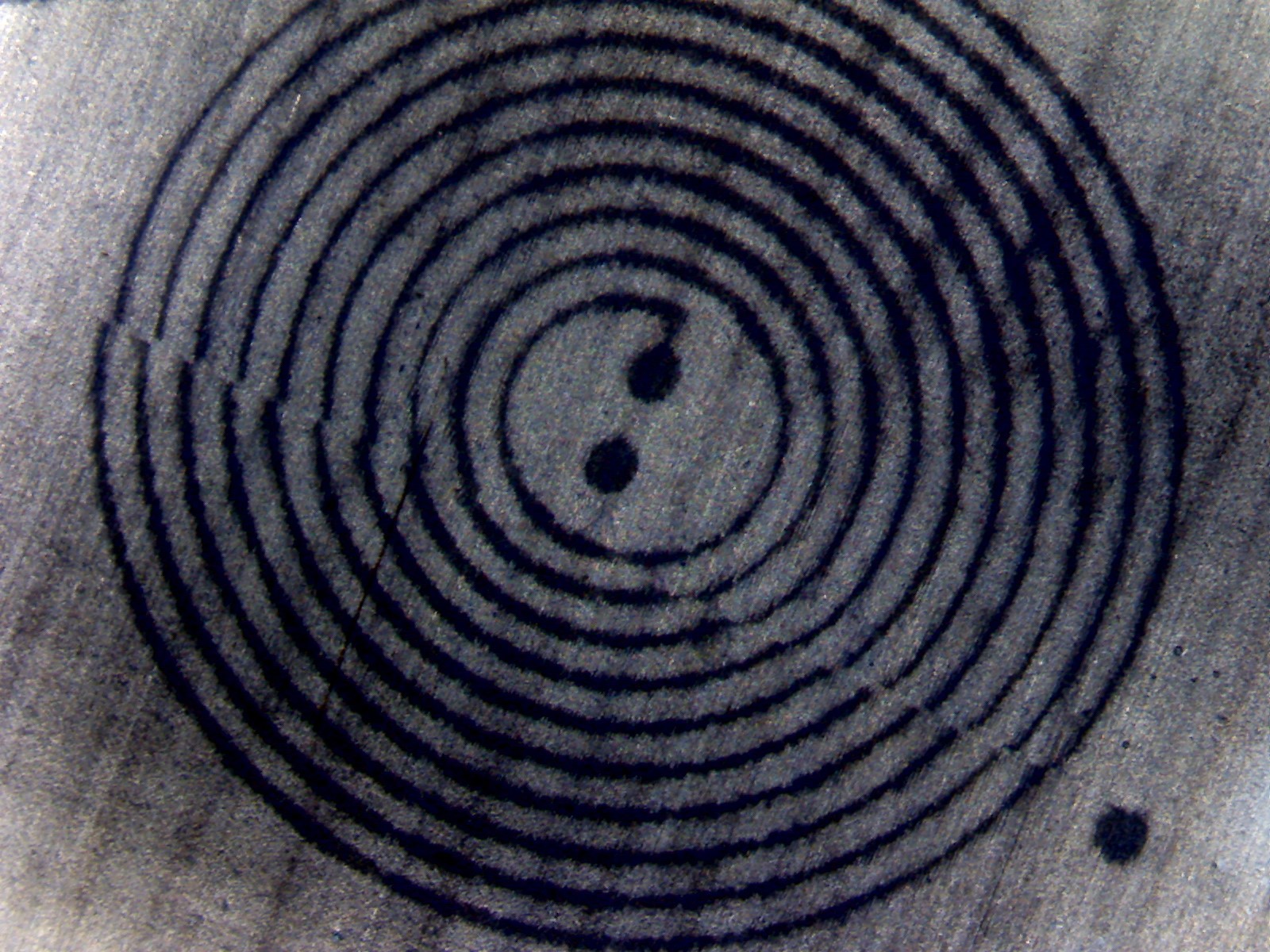
In the following picture, you see a close up of a Bugeja coil, spacing between tracks is 150 microns.
There is a mismapping of 0.16 mm between reality and board (probably needs scaling factor) You can see this discrepancy back in the board.
Discussions
Become a Hackaday.io Member
Create an account to leave a comment. Already have an account? Log In.