Jorj Bauer
-
Day 5: Stop. EEPROM time.
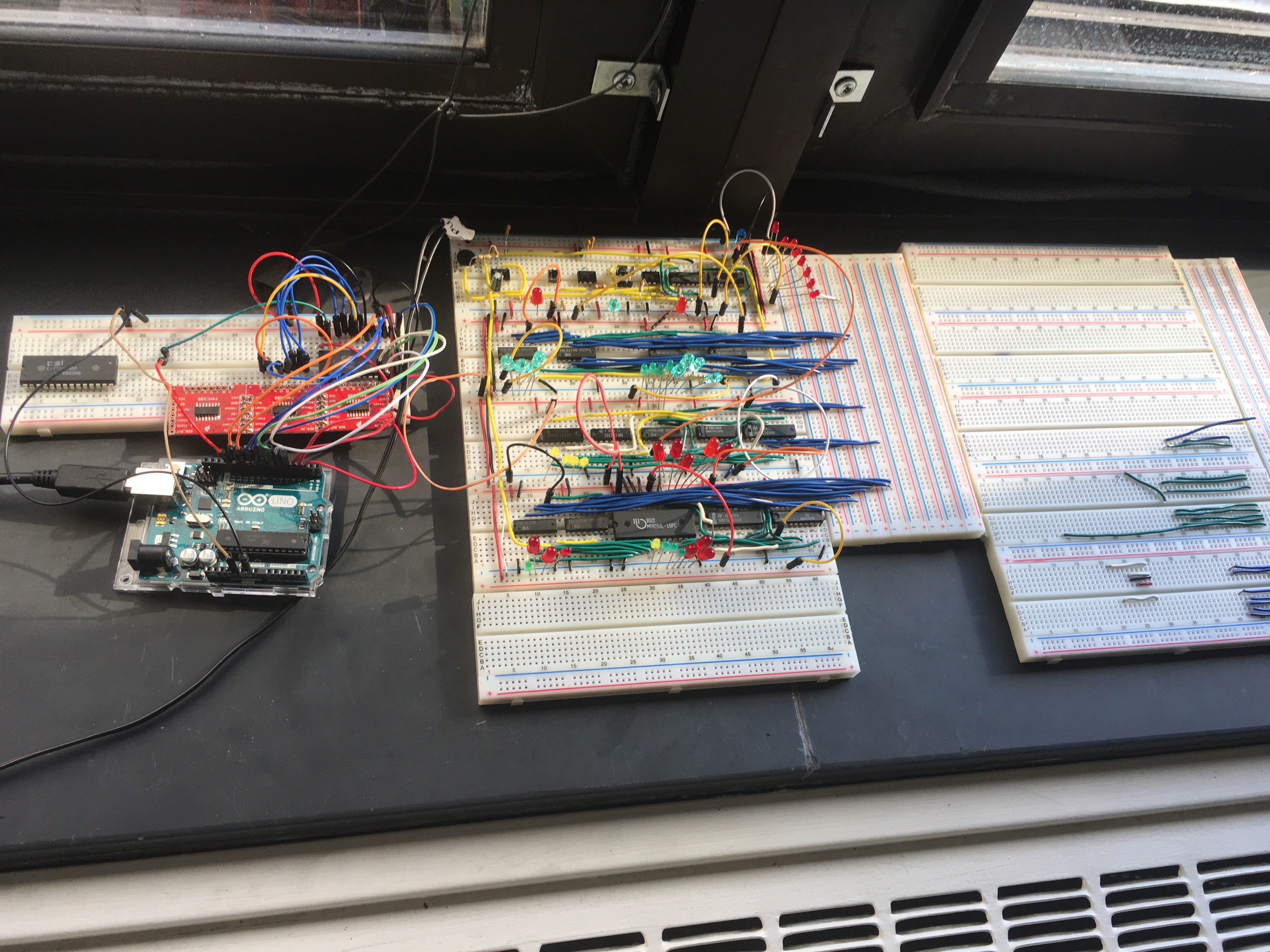
05/20/2017 at 11:51 • 0 commentsThis is the day 3 build picture again, where you see two EEPROMs sitting unwired at the bottom of the board:
![]()
These are clearly salvaged from something. One is marked so that they can be easily identified and put in the correct places in whatever I pulled them out of. Which means they've been programmed. Which raises one additional question in the "how am I going to use these?" camp.
It's not a given that they'll be usable.
Presumably, whatever device they came from was using them as updatable storage. So they probably do work as such. Sometimes manufacturers have funny tricks they can play for their customers, though: custom settings in the hardware that make it not quite adhere to the datasheet specifications. And I wonder if that's going to be the case for these.
Normally, when you write to an EEPROM, you can simply set the data lines correctly and a byte gets written. There are optimizations for writing multiple bytes at once, but they're just an extension of that model. But there's a way to further protect the contents of the device.
It took a little work to find the exact datasheet for this manufacturer, but it confirms that these have a software protection mode. If you write special bytes to certain memory locations in a given order, it activates this mode - where, if you want to write to the device again, you have to go through another little dance (figures 9 and 10). Whether or not these two chips are protected that way, I don't yet know. So it's time to build an EEPROM programmer to find out.
I grabbed an Arduino Uno and some already-chained 'HC595 bit shift registers to cobble together a clone of the EEPROM programmer that Ben Eater built. You'll see three 'HC595s on mine, here on the left:
![]()
... that's not because I needed them. It's because I had those wired up from another project. If you only need two, you only have to pay attention to the first two chips in series. Which is what I'm doing.
The EEPROM you see on the left is not connected. There's another under the mass of wires, and with a little debugging of my messy wiring, I can confirm - both chips are programmable. I did throw the "software protect disable" commands at both of them, but I don't actually think they were protected; I think I was just fighting a bit of a wiring problem.
No matter! We're off to the races.
Now, before I call this day done: I've obviously built out the boards a little. This goes hand in hand with some planning about what's going to go where so that I can place an order for the parts I'm going to have to *sigh* BUY, because I don't have the right pieces in my junk stock at all.
Notable ICs I'm going to need to order:
One adder. I have one 74LS83, which gives me 4 bits of adder. I need another 4.
A pile of bus transceivers. I've only got one more 4-bit bidirectional transceiver; I'm going to need many for the ALU that I've designed. Which will be total overkill of course. :)
Two XORs. Only because I want an XOR assembly instruction in my computer. For no real reason other than a love for completeness. I have AND and OR gates; I want XOR too, and don't have the gates to craft it out of my supplies.
A good number of LEDs. As you can see from the RAM output section, I've started having to mismatch the LEDs; my LED bin is almost empty! I never thought the day would come. I'm partial to 3mm LEDs these days, so I'll order three different colors, 16 each, which might be enough for this project.
One 1-megaohm potentiometer. The small black trim-pot on my clock board is 10k ohms. That doesn't give me a lot of variation on the clock speed, and I'm finding myself replacing capacitors to change speed while playing around. I would like that to be more flexible, and I don't have any potentiometers sitting around that are in the mega ohms range.
Some more EEPROMs. I had thought I'd make this a Von Neumann architecture machine - where the program and data are both stored in the same memory space in that 8k RAM chip. But having only an 8-bit bus means there's a bigger challenge here: if I enable the high 5 bits of RAM through an off-the-bus "PAGESEL" kind of instruction then I'd be able to address the RAM fine... but it will be tricky to change pages, keep the program running, and have all of the data that the program needs in the same page with the code it's executing. It would certainly be possible but this feels like a complication I don't need or want.
Which leads me back to the Harvard Architecture, where the program and data spaces are totally independent. It's much more tractable to deal with RAM pages separately from code pages. I could use the other RAM I've got for the program space, and add some toggle switches and buttons to manually input data. That also sounds like complication I'm not looking for. I would like to be able to program this thing, have it run, turn it off and on again, and still have it run. So I'm going to need at least one EEPROM to hold the program.
But I've got two! Which would be fine, if there were only 8 different actions that could be performed in hardware (actions like "put the RAM contents on the bus" or "store the bus contents in Register X"). A quick count shows I've got 15 different actions in my plan. I could come up with some clever 555 timer hack, driving a bit of EEPROM address space and enabling one of two output latches with 8 bits of EEPROM output; then a second 8 bits of EEPROM output. And again, that sounds like it's just a little out of reach with the parts I've got in the bin.
So: two EEPROMs will drive the control logic; another one for the program. Check.
And last but not least: two magnitude comparators. I want a comparison function that sets the Carry status flag in a way that can be used for conditional branching. Which means I need comparators to tell which of the registers being compared is greater.
Okay. Order placed. This sits for a few days and I'll design the ALU, instruction set, and microcode while I'm waiting...
-
Day 4: a bit (or eight) of RAM
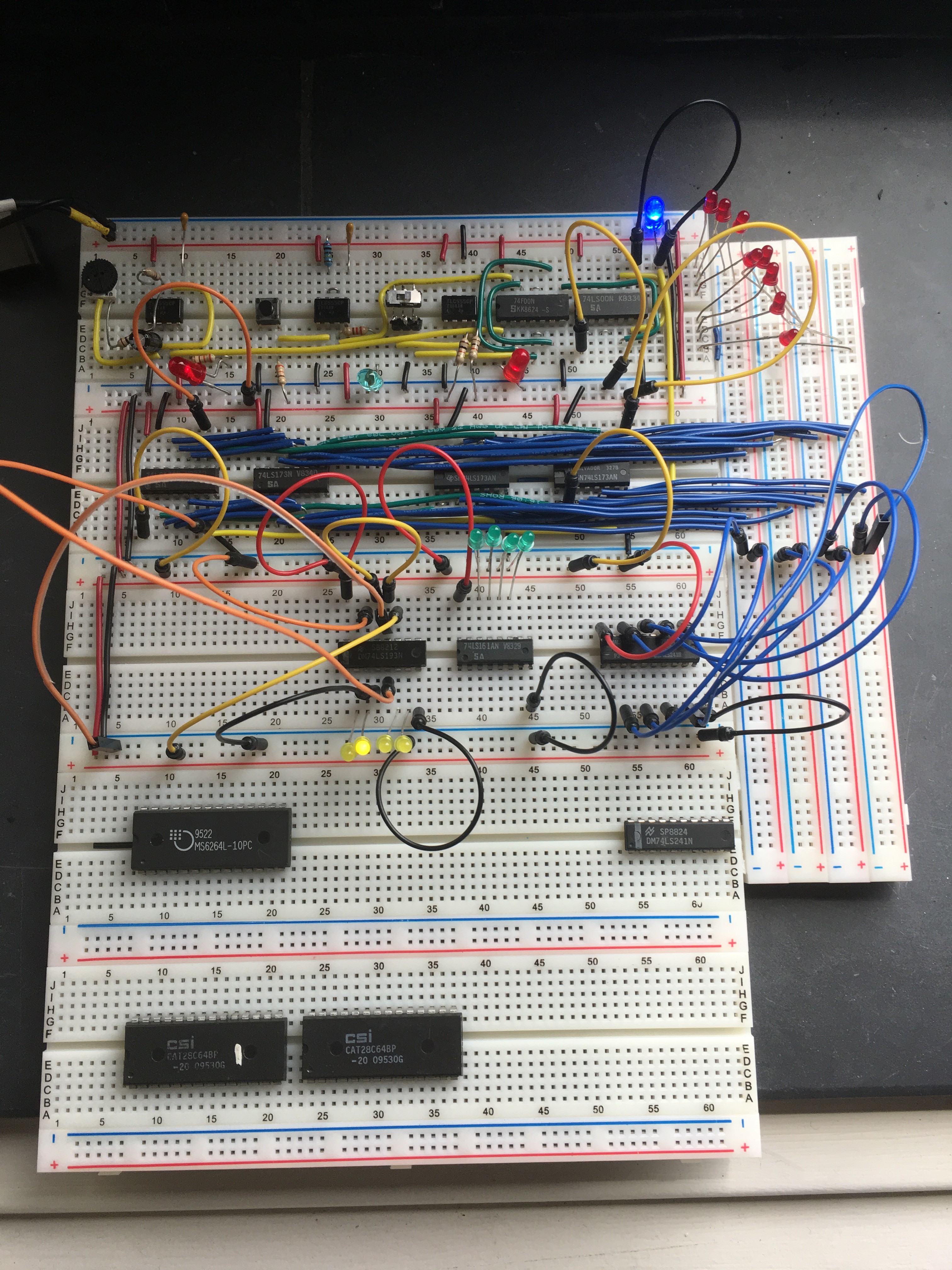
05/20/2017 at 11:13 • 0 commentsSee that MS6264 sitting by its lonesome on the left under the program counter? Well, it's 'bout to have something to do.
![]()
The MS6264 is a 64-kilobit static RAM. I found two of them in my stockpile (salvaged from old GatorBoxes, I think, along with the EEPROMs and a pile of 68000s). I would like to be able to address all 8k of it, one 256-byte page at a time - but let's start with just 8 bits of address space. That's one 256-byte "page" of memory.
I've only used one bus transceiver so far because I've only really needed to buffer the program counter output from the bus. Here, I'm going to need an input and output tri-state buffer, because I might be reading from the RAM (output *to* the bus) or writing to the RAM (input *from* the bus). This would be the perfect use of a '245 -- an 8-bit transceiver that has a simple direction setting bit. But I don't have those lying around. What I do have is two '241s; one '367; and one '244. Each of those is a 4-bit bidirectional switch (or an 8-bit unidirectional switch) so I'm going to need two. I guess the best way to deal with that is to reclaim the '241 that I just used for the program counter, replacing it with the '244; and then using the two '241s for the RAM.
The difference between the '244 and the '241 is minor. If you look at this datasheet for the 74x24x family of buffers, section 8.1 shows the differences -- on the '241, the 1G enable line is active-low while the 2G enable line is active-high. On the '244, they're both active-low. Which means that the 7404 hex inverter is no longer necessary for the PC counter output - bonus!
Staying with that 7404 inverter for a moment: instead of pulling it out, there's actually another use. The clear lines for the program counters on the two PC counter chips are also different logic senses. I'd like to have a power-on reset that explicitly holds them at "reset" while the power stabilizes - along with keeping the clock output halted - which means I still want that inverter there. Oh well.
Back to the RAM, then.
Two '241s, one 8k RAM chip with the high 5 bits tied to ground. The RAM I/O pins go to the '241s, which are wired as 4-bit bidirectional buffers. But where do the address lines come from? How do we select the address of RAM that we want to store or fetch?
I guess we're going to need another 8-bit register to store the current memory address. I have more of the '173s, so they'll do just fine. And they should also feed from the bus, so that we can set them...
![]()
And *poof*, one RAM module wired up. There's an enable line to load the memory address register from the bus; an enable line to connect the RAM module to the bus; and a RAM write enable that's tied directly to the enable that inputs RAM from the bus. It's a heck of a lot of wire in a small space, but it works...
-
Day 3: Setting and Resetting
05/19/2017 at 11:17 • 0 commentsDay 2's fun ended with an odd counter problem - where the carry from the low 4-bits of the program counter is being applied to the high 4-bits one clock cycle too early. As fun as it is to count "14, 15, 31, 17, 18" I'd much rather that my computer counter "14, 15, 16, 17, 18" like all the other computers. So my task for today, then, is to delay the application of that carry bit by one clock cycle.
The DM7474N is a dual D-type flip-flop. It's easy to use a D flip flop as a 1-bit, 1-cycle delay. (I had indeed forgotten that the 'D' stands for "Delay", even. Thanks Google.) But instead of that, here I grabbed a DM7476N dual J/K flip-flop, and convinced myself that I remembered how to use one as a delay instead of a D-type.
![]() After about a half hour of confusing the hell outta myself, I went back to the obvious choice and built it out of a 7474. :)
After about a half hour of confusing the hell outta myself, I went back to the obvious choice and built it out of a 7474. :)Now the counting logic looks like this, with the flip-flop delaying that low carry by one clock cycle:
High bits D Flip-Flop out ("Q") D Flip-Flop in Low Carry Low bits Output 0000 0 0 0 1000 8 0000 0 0 0 1001 9 0000 0 0 0 1010 10 0000 0 0 0 1011 11 0000 0 0 0 1100 12 0000 0 0 0 1101 13 0000 0 0 0 1110 14 0000 0 1 1 1111 15 0001 1 0 0 0000 16 But there are *two* new ICs in the clock module. What's the other one?
I played for a little while with reversing the two ICs - using the '193 as the low bits. Immediately there's a problem, because the carry out from the '193 is active-low. So I needed an inverter while playing with that configuration. The MM74C04N from my pile of parts did just fine.
I've also connected the output of the full 8-bit program counter to the bus using one '241, which is seemingly designed as a bidirectional 4-bit bus interface (not a unidirectional 8-bit bus interface). The two separate enable lines on the '241 have opposite control logic: one requires a low signal to enable, and the other requires a high signal. If you were using this as a bidirecitonal 4-bit control, you could tie together the two; if the logic were high, you'd be flowing in one direction across the chip and when you switched to low, you'd be going the other way.
Since that's not what I'm doing - I only care to gate the output, tri-stating *to* the bus, not worrying about what comes *from* the bus just yet - I should probably tie those two together to one control line via an inverter. So it's wired to the hex inverter '04; when one line is low, the other is high, and I can turn this on and off as a single unidirectional 8-bit switch with just one control line.
-
Day 2: The Island of Misfit Counters
05/19/2017 at 03:27 • 0 commentsProgram Counter! The computer needs one of these. It keeps track of what memory location is going to execute next. Should be pretty straightforward: it needs to (a) store an 8-bit number; and (b) increment it on demand.
I guess I'd like to be able to branch, which means I'll also need to be able to (c) arbitrarily set it to a new value.
This is going to be interesting.
It would make sense to build this out of two counters; where the "add 1" instruction comes from the CPU's control logic ("hey, I just read from program memory! Increment now please"). But I don't have any two matched counters: I have two different unmatched counters.
I have one 74LS161AN, a synchronous 4-bit counter; and one DM74LS193N, a Synchronous 4-Bit Binary Counter with Dual Clock.
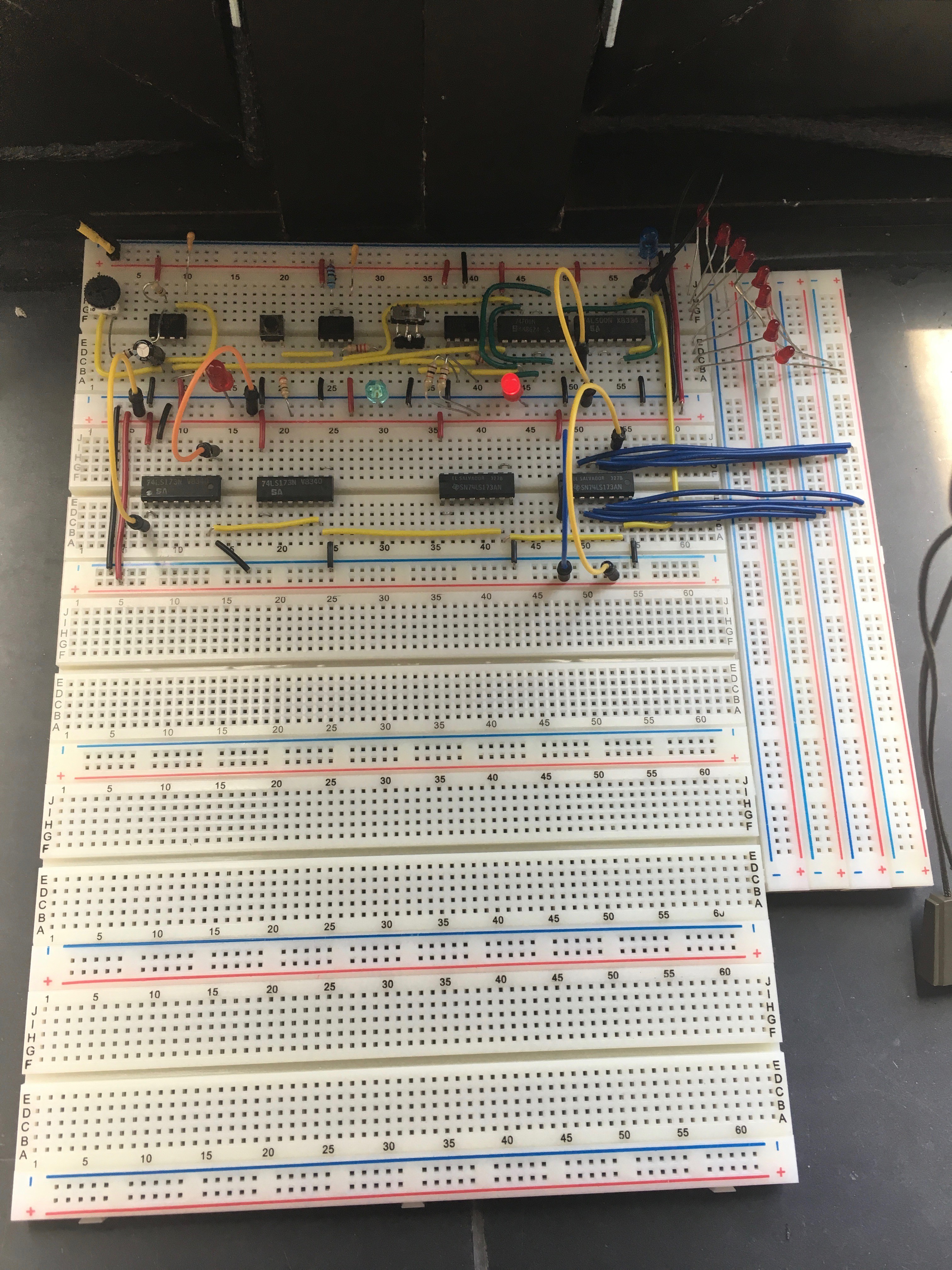
![]()
This picture is from testing how those are going to work. Also: I've obviously selected one RAM chip, picked out two bus drivers, and set aside two EEPROMs. Ignoring those for the moment, let's stick with the counters.
The counter on the left, shown here with the lit yellow LED under it, is the '193. The '161 is a clocked adder, perfect for the job I want to do; while the '193 is an unclocked counter with both an "increment" and "decrement" line but no explicit clock. Not a big deal. If I use the '161 as the low order 4 bits, then its carry-out can trigger the '193's add. Easy peasey.
Except for one minor bit: the "carry" line is set high on the '161 when all of its outputs are 1. That is, the carry is set the clock cycle before the '193 needs to increment. If these were two '161s, this would mean that on the next clock cycle's rising edge, a second high-order '161 would notice that the carry-in flag was set and increment. But since the high order bits are a '193 and it's not clock-triggered, it happens immediately.
That means that these two counters count together like this, in binary, from 8 onward:
High bits Low Carry Low bits Output 0000 0 1000 8 0000 0 1001 9 0000 0 1010 10 0000 0 1011 11 0000 0 1100 12 0000 0 1101 13 0000 0 1110 14 0001 1 1111 31 0001 0 0000 16 Whaa? 13, 14, 31, 16, 17 ... obviously not what you'd expect - but because the carry bit is set whenever all of the low bits are on, and the '193 performs that action immediately instead of waiting for the next clock pulse, that's the way it plays out with this pair.
Now, technically, I don't have to fix this. We could just say that this is the order in which instructions are run. It's not intuitive, and would certainly cause some headaches while trying to program the computer; but as long as the sequence is deterministic, there's nothing stopping us from using this very odd counting scheme. The last byte of the next 4-bit memory half-page is used first, that's all.
I'm confused just trying to write it down.
So no, obviously I'm not going to do that. Instead let's add a little bit of complexity in the electronics to bring back simplicity to the counting. Tomorrow.
-
Day 1: taking stock
05/19/2017 at 01:32 • 0 commentsMy plan here is to do this build primarily at work, during my lunch hour. To do that, I need some idea of what I'm building; and a reasonable set of parts out of which to build that thing.
Well, I know what I want to build, sort of. The recently popularized Ben Eater 8-bit computer videos made me think about building something similar. So that's easy. Ish.
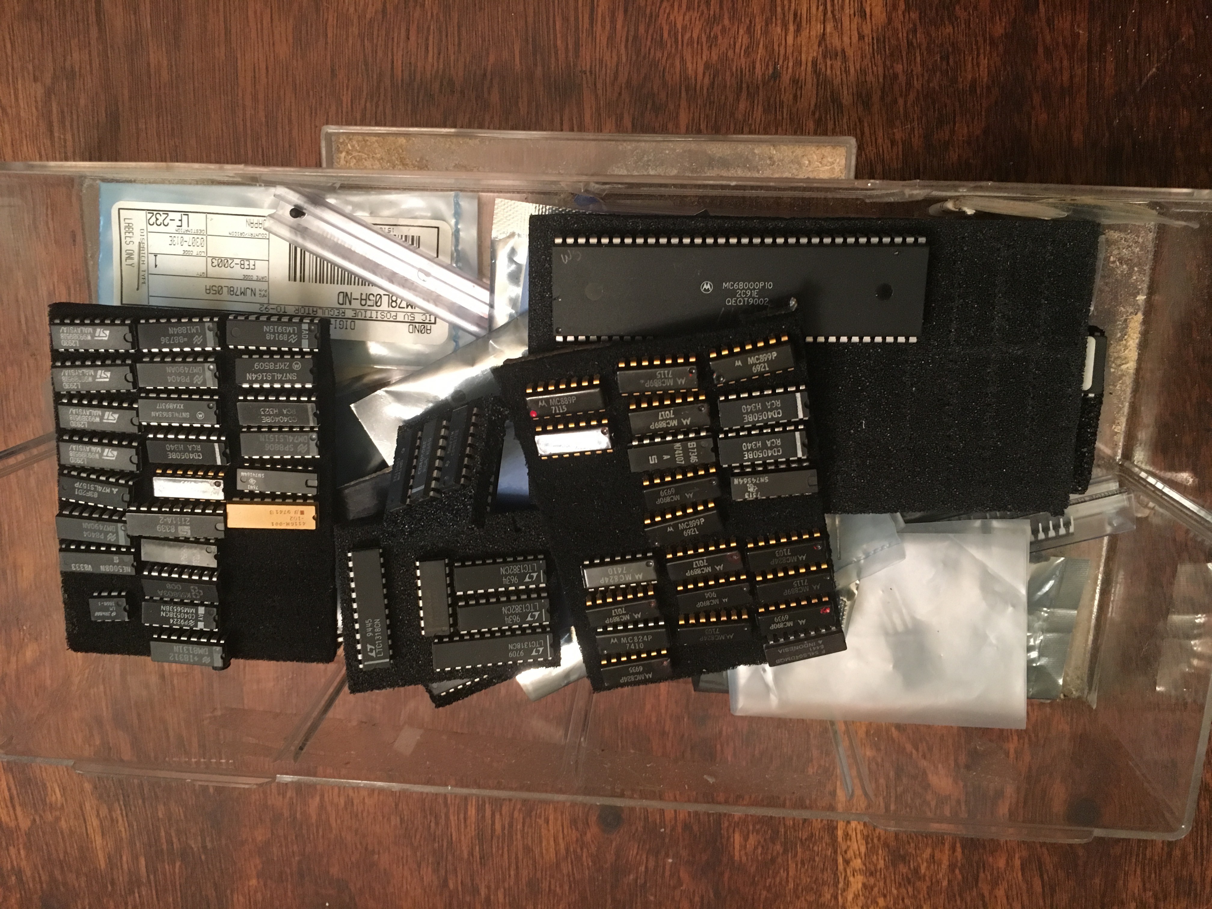
But what, exactly, do I have? Well, here's some of it. The static foams are loaded on both sides with ICs...
![]()
Ignoring the families (many of these are TTL; some are the LS family, and others are not; some are CMOS; etc.) -- and just cherry-picking the parts that look interesting and possibly useful:
6x 7400 quad 2-input NAND gates
1x 7402 quad 2-input NOR
5x 7404 hex inverter
5x 7405 hex inverter
1x 7406 hex inverter
1x 7407 hex inverter
1x 7408 quad 2-input AND
1x 7410 triple 3-input NAND
1x 7420 dual 4-input NAND
1x 7421 dual 4-input AND
1x 7448 BCD to 7-segment driver
2x 7427 triple 3-input NOR
1x 7483 4-bit adder w/ fast carry
2x 7432 quad 2-input NOR
1x 7490 decade counter
1x 74135 1-of-8 decoder
2x 74138 1-of-8 decoder
3x 74139 dual 1-of-4 decoder
7x 74173 4-bit d-reg tri-state
3x 7476 dual j/k flip-flop
1x 7474 dual d-type flip-flop
2x DM7446 BCD to 7-seg driver
1x 74174 hex? quad? D-type flip-flop
2x 74153 dual 4-input multiplexer
1x 74193 4-bit up/down counter
1x DM7489 64-bit RAM
1x 74367 hex 3-state buffer/bus driver
1x 74109 dual j/k flip-flop
1x 7475 4-bit bistable latch
2x 74151 1-of-8 selector
1x 74161 4-bit counter
2x 74241 octal tri-state bus driver
1x 74244 octal tri-state bus driver
2x MS6264L-10 static RAM (64k bits)
2x CAT28C64B-20 EEPROM (64k bits)
5x 555 timers
1x 7474 D flip-flop
1x MSM2114 4k static RAM
2x 211A 4k static RAM
6x MC824P quad NOR gates
1x CD4016 quad bilateral switch
1x CD4053 analog 8-channel multiplexer
1x 74157 quad 2-line to 1-line data selector/multiplexer
1x DM8131 6-bit bus equality comparator
... that certainly looks like a good catalog of parts to start with. I'm sure I'll want to order some new parts along the way, but if I use many of those parts that have literally been sitting in my basement for over 20 years, I'll feel like something was accomplished.
Some ground rules for myself, then:
First try to use parts I already have.
If I have to order something, I will - but only the minimum necessary. I want to end this with smaller stockpiles of parts in my basement than when I started.
I would like this to eventually do something interesting. If it only blinks some LEDs, I'll take it. But more is more betterer.
16 protoboards ordered, then! And now it's time to get started.
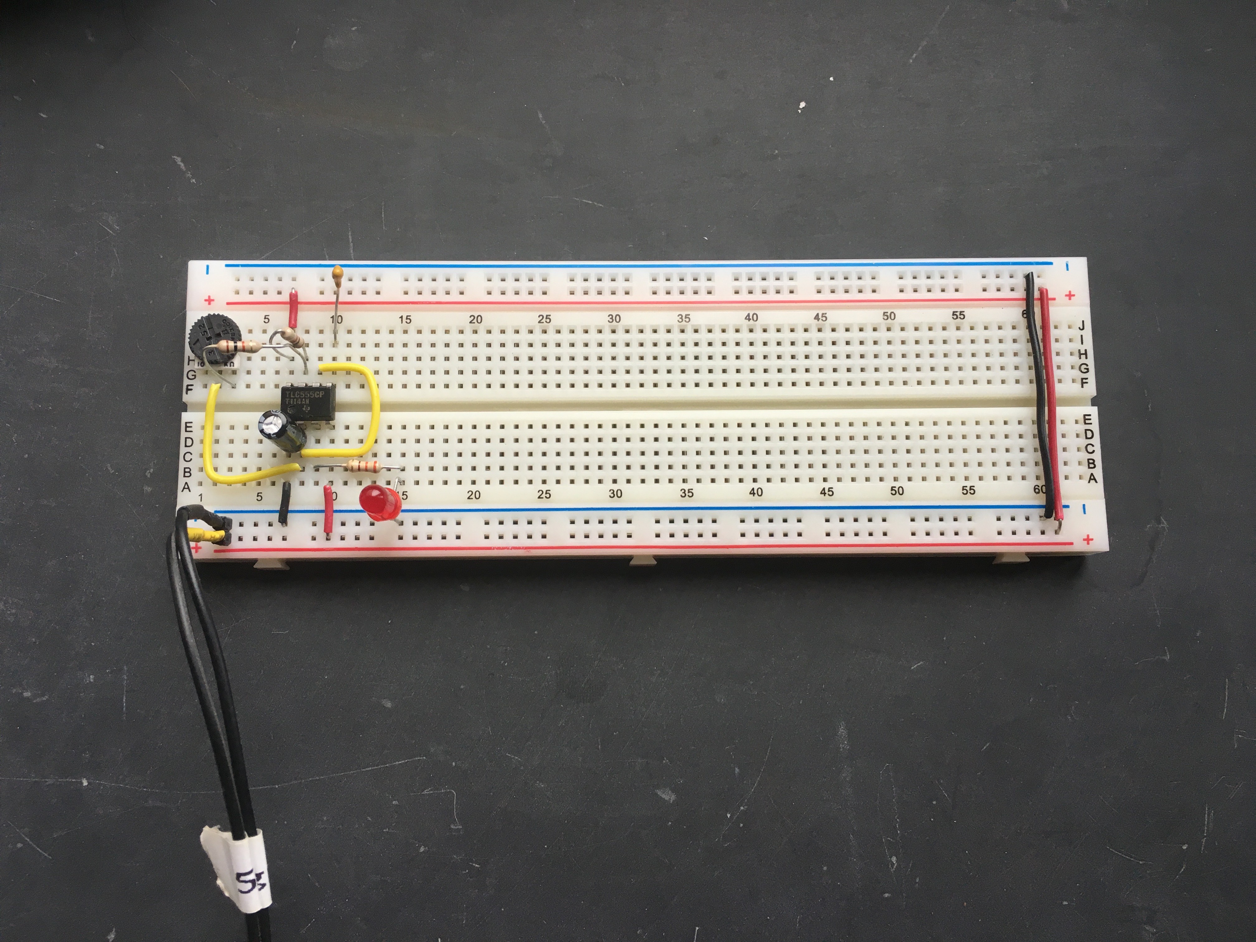
In Ben's series, he started in a very sane place - the clock. So did I, more or less using his design. Not much to say here; if you want to understand how this works, go watch Ben's videos on the subject. I substituted logic gates that I had lying around, of course; two 7400 series NAND ICs used, along with 3 555 timers. Here it is as the first timer shows that it still works...
![]()
It quickly grows, taking on four of the 74173 4-bit registers, making what I think will be an X and Y register. This is more dead-simple read-the-datasheet kind of work and I don't think it needs much description - except to say that I'm a big fan of the 6502 instruction set (my first assembly) and I'm definitely thinking in its terms. Maybe this has too many registers when it's done, but I would like an X/Y and Accumulator...
![]()
There's just enough wiring to test whether or not that first (last? rightmost?) register chip still works. So far, so good - no duds in my stock! We'll see where this goes tomorrow, and in a few days I'm expecting a logistical puzzle or two...
Detritus, the 8-bit ... computer?
I have a lot of random spare parts doing nothing and a need to make them do things...

 After about a half hour of confusing the hell outta myself, I went back to the obvious choice and built it out of a 7474. :)