The PCB has undergone some revisions since I've started the project:
Version 1 was the first board ordered from oshpark:
This board works OK, but had a few issues:
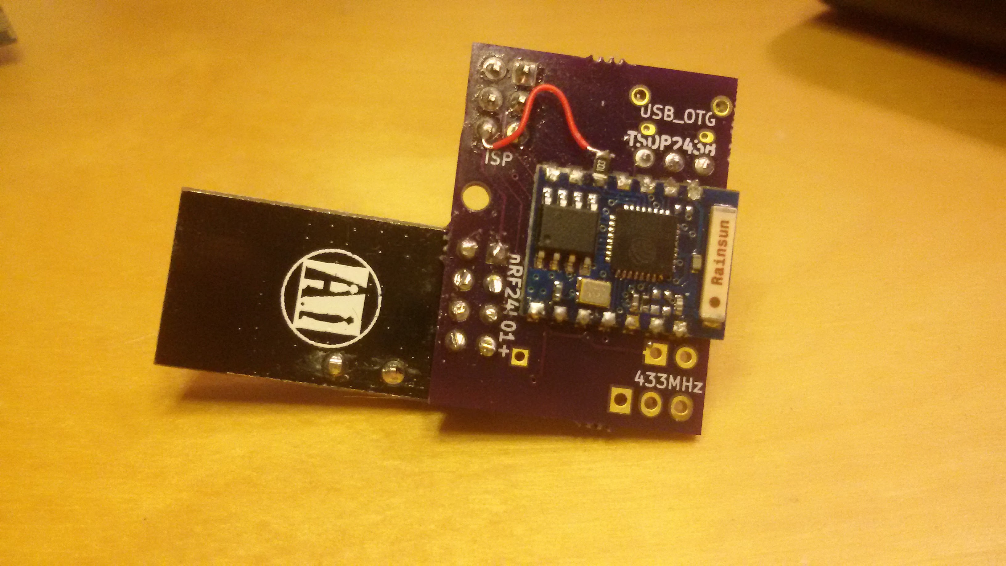
- I had forgotten to pull down GPIO15 on the ESP. This means the module won't boot properly and this had to be fixed with a patch wire
- I used a TSOP2438 footprint for the IR receiver, but I found out I had a HS0038. This meant I had Vcc and GND reversed. This was easily fixed by bending the pins on the receiver and adding some heat shrink to prevent shorts.
- The micro-USB-B connector is supposed to stick out about 1mm from the board, but I had aligned it with the edge. This meant that the connector is pushed up a little at the edge.
- The 433 Mhz transmitter was powered from 3.3V regulator. Presumably 5V would give better signal and from previous experiments I knew I could power it at 5V and still signal it from 3.3V.
- Some weird conflict occurred between the ams1117 on my PCB and the one on the USBasp AVR programmer, which broke the 3.3V power on the USBasp. All of this happened with no power applied to the spider board.
The patches are visible in these images:
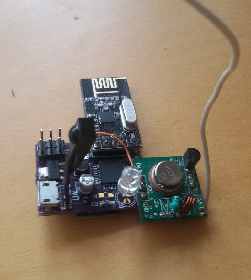
Version 2 has a few improvements:
- GPIO15 pull down, 5V to 433Mhz transmitter, IR receiver and USB connector issues were fixed
- More AVR GPIOs were broken out to a header, including the uart IO lines which make it possible to also flash the ESP through the header
- The 5V is now also available there. This made it a lot easier to connect a PIR sensor. In version 1 I only had 3.3V available on the header, which meant I had to bypass the regulator that is normally present on the PIR sensor module.
- The header is now female, so that I can push some extra long pins in the header for AVR programming. This way I can leave out the Vcc pin which in turn means that the power on the board and the (new) USBasp are no longer connected.
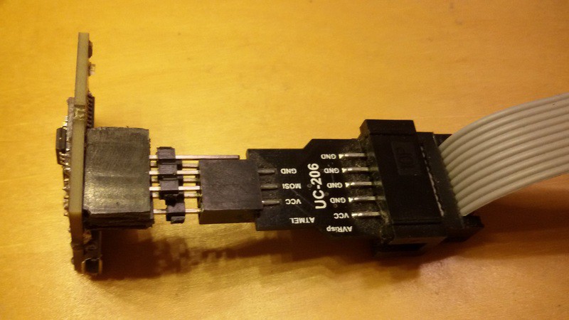
The following picture show the setup for programming the bootloader into the AVR. If you look closely, you'll see that the Vcc is disconnected. Also visible is the USB connector on the bottom that now extends from the PCB.
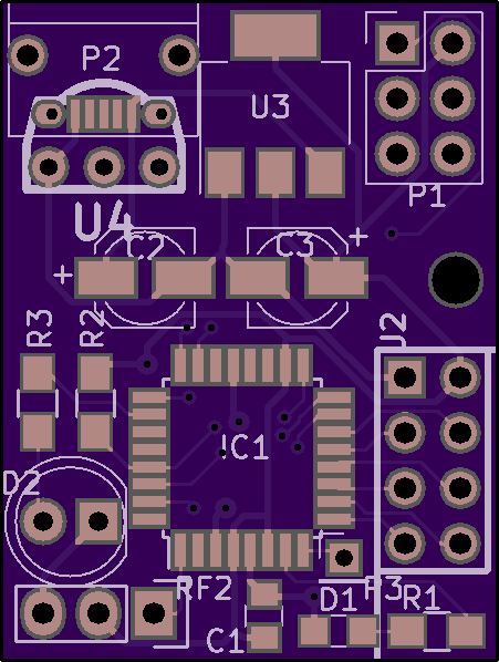
Small adjustments are still made to the design although I haven't ordered new boards of this revision yet. The most notable change is that I'm now including small solder mask lines between the pads of the atmega. This should make it a little bit easier to solder the pins of the TQFP package.
Discussions
Become a Hackaday.io Member
Create an account to leave a comment. Already have an account? Log In.