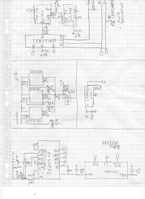
I'm Not normally into making quick updates, but I have updated the schematic to be a little more in line with what I was thinking. When I went through the caves for a good ideal diode I found I could replace quite a few parts in one go. Most of the darlington PNP transistors can be removed, and almost all the protection diodes could go since their voltage drop would most likely push this out of spec, and all those devices functions was covered by this singular chip. It can carry 2.6 amps, and it's dropout voltage is lower than the diode and the transistors. The schematic looks off in my head. It's like there are too many parts between the boost converters and USB ports, but I will figure it out. I didn't bother mucking with the microcontroller and logic circuitry. I just made a point it exists with the 3.3v regulator. I will try to run a simulation on this before I order it.
***ERRORS***
- The resistor values for the enable pin of the boost converters are too high. The value that I am looking for is 600 Ohms.
- There is very little over voltage protection circuitry on the input side of the USB. It connects directly into the 5v rail with only a "diode" in the way. I'm not too worried about this one though. It won't greatly impede any testing.
I will have to post a new circuit.
 Krinkleneck
Discussions
Become a Hackaday.io Member
Create an account to leave a comment. Already have an account? Log In.