The term "High Speed" is often misinterpreted as if it relates to the frequency of a signal which indicates how often the signal repeats itself. In fact, the rise and fall time of a signal is what distinguishes a high speed signal from a low speed signal.
"High Speed" is generally interpreted to mean circuits where the length of the signal’s rising or falling edge is greater than about one-sixth of the transmission line length.
Key Words: rise and fall times, eye diagrams, gate input and output impedance, transmission lines, latency and timing issues, electromagnetic interference, packaging issues, thermal management, terminations and vias, power and ground planes, clock distribution, signal launching, substrate materials, and test and measurement issues.
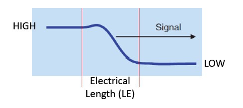
The figure above shows the transition of a signal from HIGH to LOW. The length of transition is called the electrical length (LE) and if the one-sixth of the LE is:
- less than the transmission line length, then the transmission line demonstrates distributed line behavior.
- greater then the transmission line length, then the transmission line length demonstrates lumped line behavior.
Wave Tank Analogy
There is a tank filled with water.
- A jug of water is poured slowly and the water level increased as a whole. In other words, the potential of the line changes so slowly that no reflections are produced. (lumped line behavior)
- A jug of water is poured quickly; disturbance is created and reflections are produced. This is a high speed effect. (distributed line behavior)
Example Question:
If line length = 100mm, rise time = 1.67ns, and propagation delay = 55ps, are the transmission line techniques needed to be applied?
LE (Electrical Length) = Rise Time * Propagation Velocity
Propagation Velocity = Propagation Delay^(-1)
LE = 1.67*10^(-9) * 55*10^(-12) = 30.36cm
One-sixth of LE = 5.06cm
Since the line length > LE/6 the line demonstrates distributed line behavior and hence TL techniques need to be applied.
Impedance Discontinuity
Changing the PCB track thickness cause discontinuity in track impedance and as a result reflections are produced in high speed signals. These reflections have a negligible effect in lumped systems whereas they are a major problem in distributed line systems.
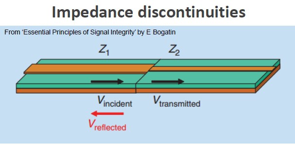
The wave-like propagation issue may be minimized by applying transmission line (TL) techniques.
- Controlled Impedance Trace Routing: Altium Designer has a routing feature which allows the PCB designer to alter the trace thicknesses such that the ringing effect is minimized.
- Termination at the Receiver: This method terminates the excess energy of the signal and prevents signal energy bouncing back and fourth.
Microstrip (Ext. Routeing) vs. Stripline (Int. Routeing)
At higher frequencies, transmission line wiring provides superior performance by minimizing crosstalk, signal distortion and radiation (as compared to ordinary point-to-point wiring). When implementing transmission lines on a PCB, there are two options: microstrip and stripline.
A microstrip transmission line consists of a copper trace separated from a ground plane by an insulating substrate. This configuration is depicted in the image below.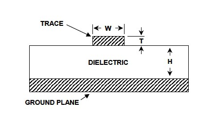
Since one side of the conductor is exposed to air, these transmission lines can only exist on top and bottom PCB layers. The trace impedance is influenced by both the dielectric of the substrate material and the air above it.
Unlike microstrip, stripline transmission lines are fully contained within a substrate – which is sandwiched between two ground planes.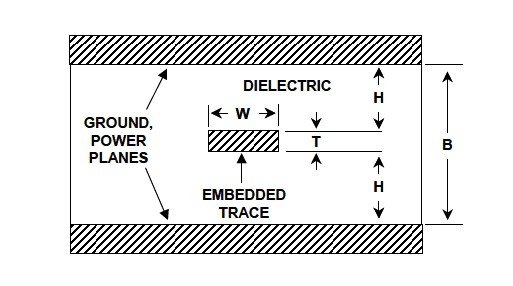
Due to the substrate impregnated nature of stripline, these transmission lines can only exist on internal routing layers and require a minimum of 3 PCB Layers (2 ground planes and a routing layer in the middle).
Change of Reference Plane or Routeing Layer
As it was mentioned earlier while designing a high speed PCB the return current path needs to be considered - if the routeing layer is changed then its return current may need to change layer as well. I will provide some examples to further explain the case but first we have to understand the different types of vias. Vias introduce impedance discontinuity and at extreme frequencies they act as transmission line stubs which are source of reflection. The figure below shows different types of vias.
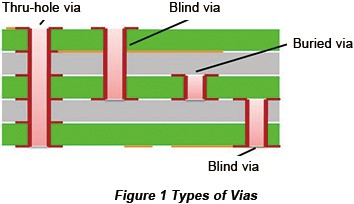
A via presents a short section of change in geometry to a trace and can appear as a capacitive and/or an inductive discontinuity. These discontinuities result in reflections and some degradation of a signal as it travels through the via. Reduce the overall via stub length to minimize the negative impacts of vias (and associated via stubs). Because longer via stubs resonate at lower frequencies and increase insertion loss, keep these stubs as short as possible. In most cases, the stub portion of the via present significantly more signal degradation than the signal portion of the via. TI recommends keeping via stubs to less than 15 mils. Longer stubs must be back-drilled. For examples of short and long via lengths, see the figures below.

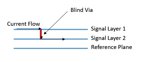
The figure below shows the first example where the routeing layer changed on the same side of the reference plane by a blind via. In this case the return current needs to change layer as well hence a second via needs to be placed near the signal via. Moreover, since the controlled impedance routing is applied, the thickness of the stripline trace (on signal layer 2) needs to be narrower then the microstrip trace (on signal layer 1).
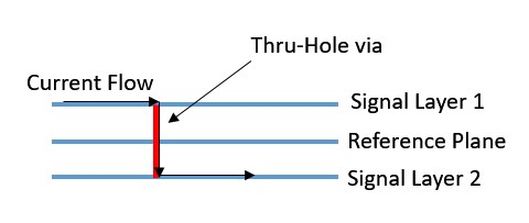
The figure below shows the second example where the routeing layer changed on the opposite side of the reference plane by a thru-hole via. In this case the return current doesn't need to change layer since the reference plane is adjacent to both of the signal layers.
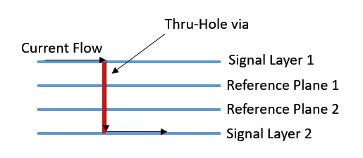
More significant problems occur when we change the reference plane.
- Change of reference plane causes skin effect which occurs when an appropriate return is not provided. This issue gives rise to poor signal integrity and high levels of crosstalk.
- A second via needs to be added for the return path which needs to be placed close to the original signal via. If not ringing effect occurs which is the reflection of signal energy.
The figure below shows a PCB cross-section where he reference plane needs to be changed.
 Timing and Delay
The controlled geometry of TLs provide predictable propagation velocity (and delay). The trace length is directly proportional to propagation delay. For example, the same sourced clocked signal may arrive at different components at different times depending on the trace length. Predictable propagation velocity allows us to control over timing skew.
For source-synchronous interfaces, the data signals must arrive at the load at the same time as the clock. This is done, for instance, by matching the lengths of all the signals between data lanes and strobes. The trace length matching is called serpentining, by doing so the delays can be matched and hence the timing skews are negligibly small. The figure below show an example.
 The YouTube video below shows how to use the serpentine tool of Altium Designer.
Termination
This is a TL technique which is based on absorbing the energy of an incoming wave to prevent reflections. Open and short circuits are perfect reflectors. On the other hand, loads that are equal to the transmission line's characteristic impedance are perfect absorbers.
The termination method improves the signal integrity (the signal's quality) and sharpens the state transitions.
Eye Diagrams
Eye diagram is a tool to analyze the quality of high speed signal over a channel. It depicts signal amplitude vs. time. Oscilloscope vendors like Agilent provide different applications for interface wise eye diagram measurements. Jitter describes variations in the timing of a signal or clock transition.
The eye should be open!
- Closed from the sides: timing problems (jitter)
- Closed from the top & bottom: signal integrity problems
- Excessive jitter and poor signal integrity causes misinterpreted logic levels.
Quick Notes for HS design
- Tight coupling of signal trace and reference plane.
- Tight coupling of power-ground planes. (enables high freq. decoupling)
- Well-implemented capacitive decoupling.
- Low inductance power distribution.
Discussions
Become a Hackaday.io Member
Create an account to leave a comment. Already have an account? Log In.