Schematic Updates
Had a sleep on the schematic issues and decided to make few changes.
- Fixed the Memory Address Register (MAR) design over kill.
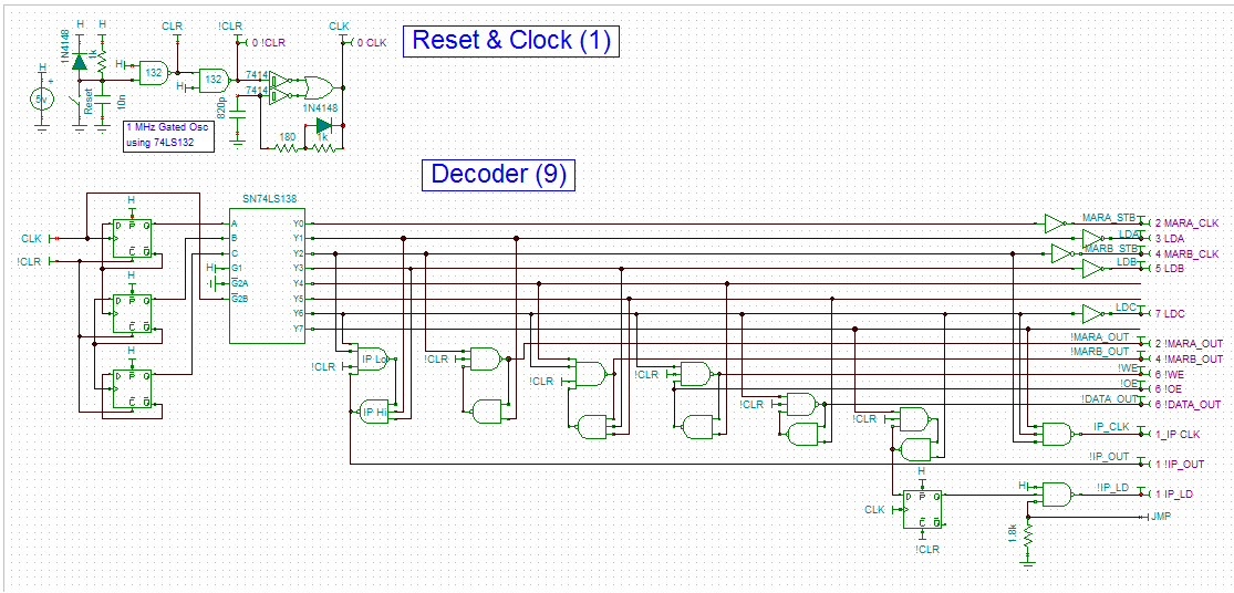
- Change the Decoder logic for 74LS373's (transparent latch) rather than 74LS374's (clocked D-latch). The reason for this is purely that the transistor count for a 74LS373 is much less than for a 74LS374.
- Reworked the Instruction Pointer (IP) for 74LS161 counters rather than 74LS83 adders. The reason for this is that I cannot initialise (upon reset) the current IP design.
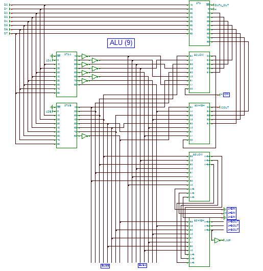
- Reworked the ALU for signed integers rather than unsigned integers (as I have worked out how to do signed integer comparison).
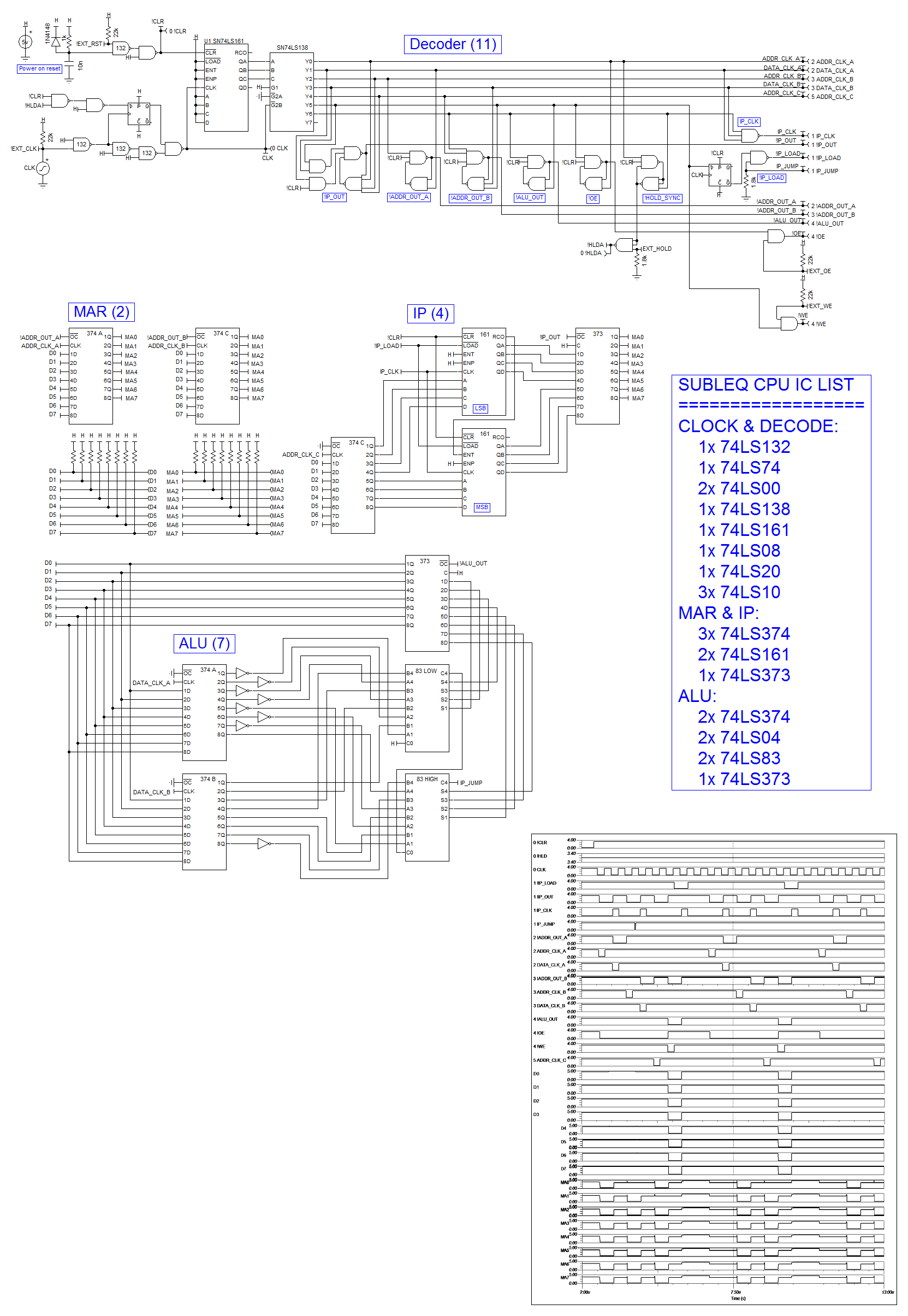
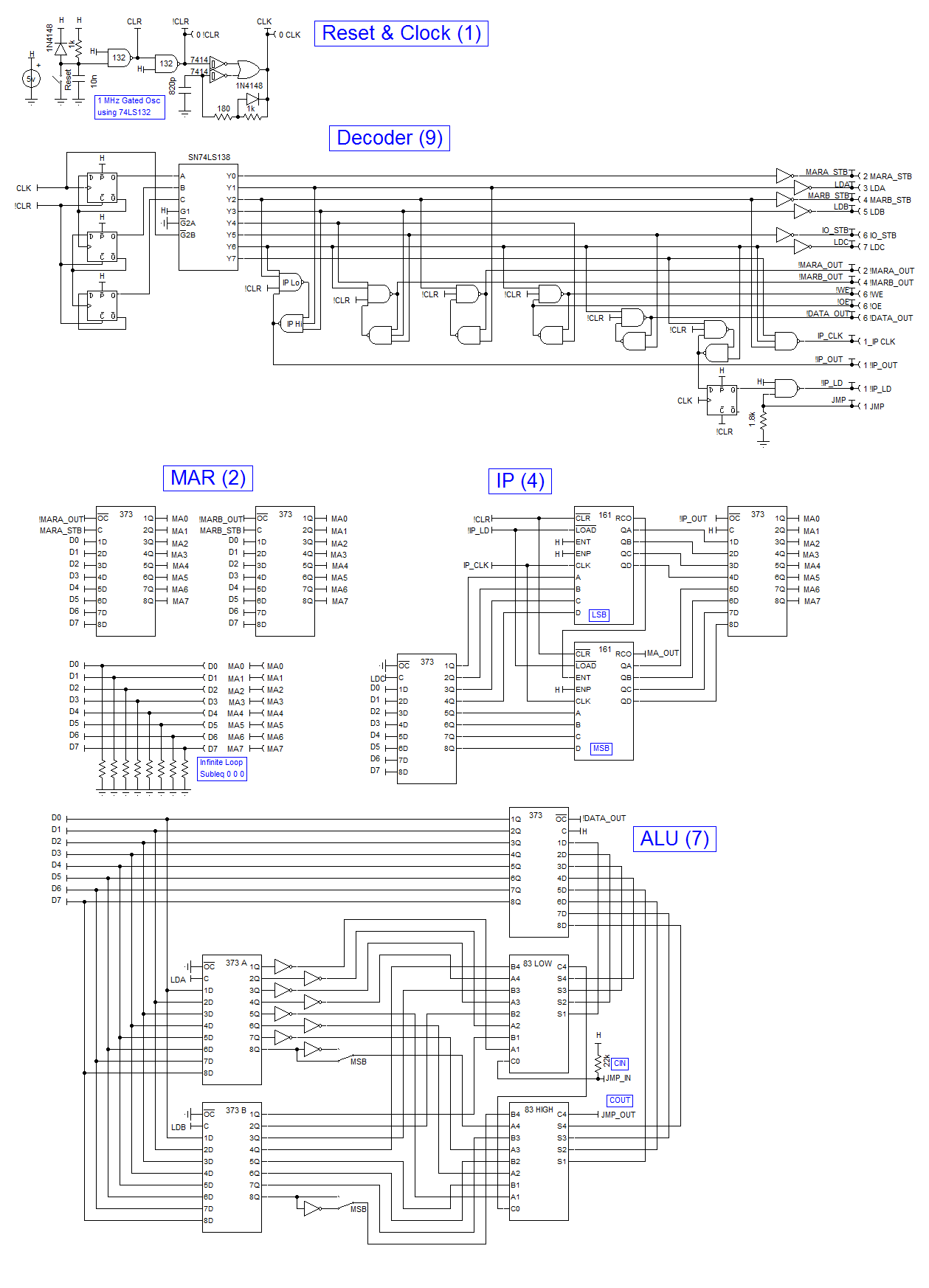
Here is the updated Reset/Clock/Decoder:
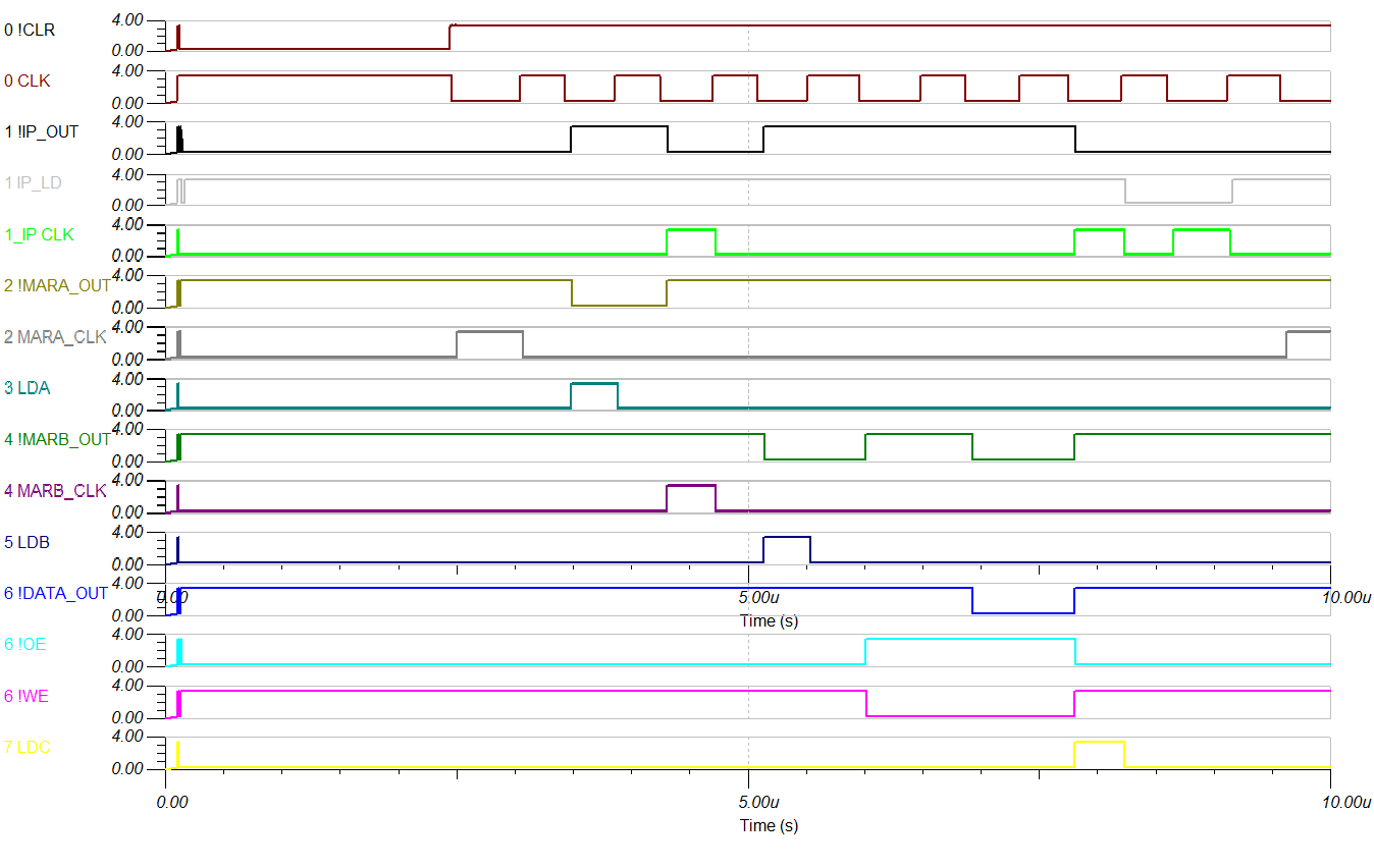
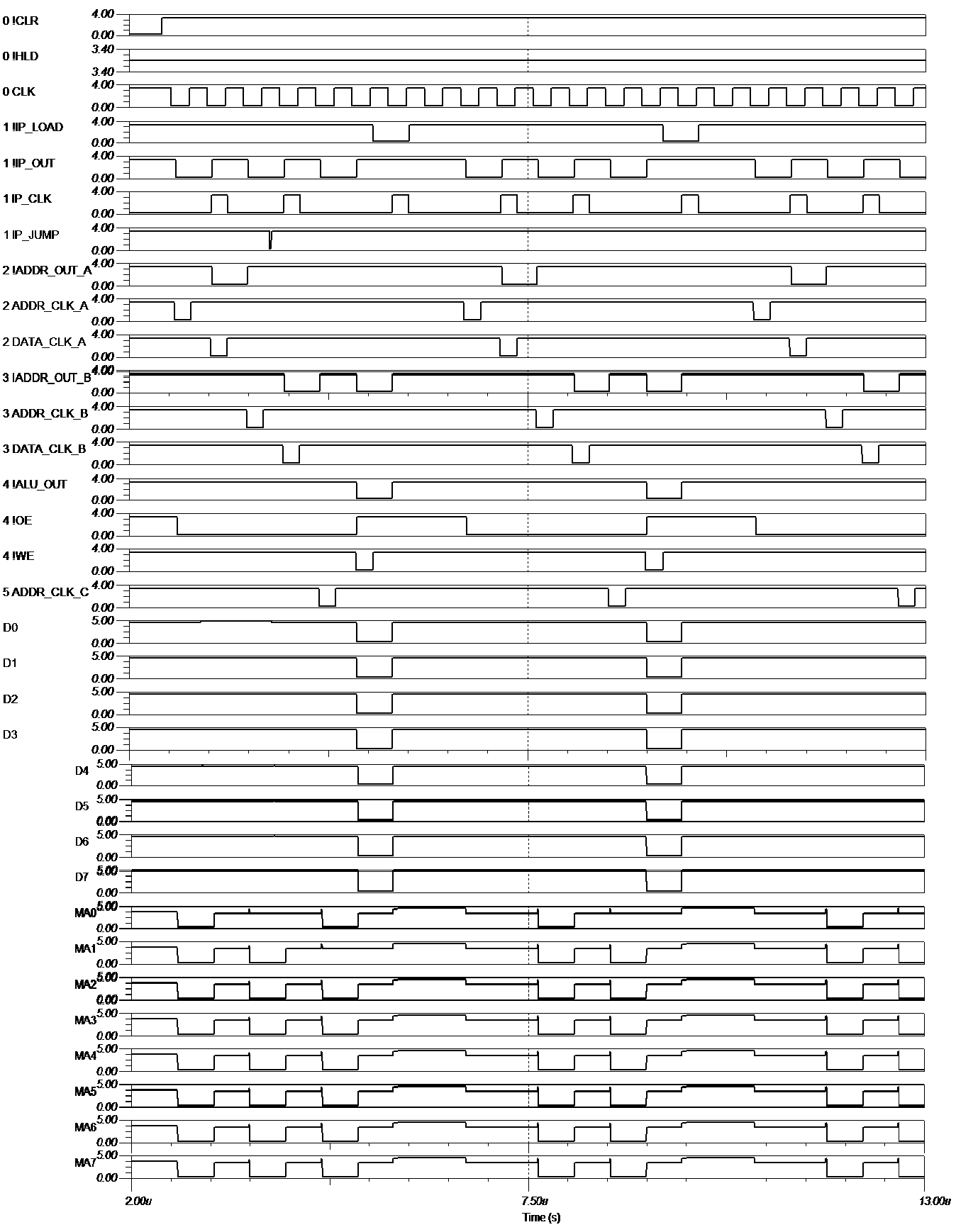
And the Timing Signals:
 Here is the Memory Address Register and Instruction Pointer:
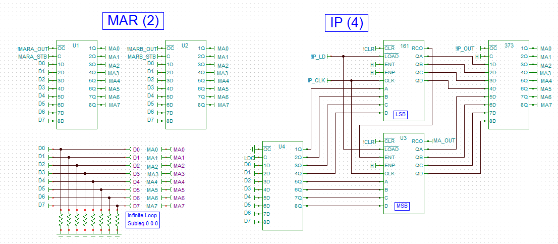
Unfortunately the 74LS373 does not seem to be working in TinaTI so I can not test the circuit(?). In theory the simulation is an infinite loop (Subleq 0 0 0). And finally, here is the ALU:
More revisions:
- Added a strobe for IO output as the memory cycle is less than ideal (for static RAM without !OE).
- Removed the ALU comparator circuit as it is redundant (at least I think it is).
Here is the updated ALU:
As far as I can work out the Carry (i.e. Borrow) is all I need!
Memory Write and Bus Conflict
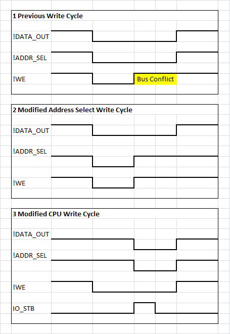
Bus conflicts are not usually a problem with simple systems as they do no damage. The reason is that TTL signals cannot supply much current (100s of uA). But an Arduino can supply ~100 mA so a bad bus conflict can do damage. I blew up my 4 Bit CPU RAM through careless testing of the memory (I have since modified the write cycle to solve this problem).
Here is the problem write cycle (1), the memory decoder fix for the 4 Bit CPU (2) and the CPU fix (3):
In case (3) the write cycle is less than ideal for latching registers so I have added an IO_STB signal o the decoder schematic (which can be inverted for IO_CLK in necessary).
PCB/Bus Planning
The problem with PCBs are:
- testing a complex PCB is hard
- schematic errors require a new set of PCBs to be manufactured (whic costs time and money)
- you get at least five copies (and you only need one that works!
So what is PCB/bus planning is about:
- splitting a complex board into several simpler boards so that it is easier to debug and only bad boards need to be re-worked. Call it divide and conquer.
- providing convenient test points for easier debugging.
- working out how to "stack" the boards (the bus) so that the spare boards are not wasted (and the complexity of each board is reduced). That is, make two 8 bit boards rather than one single 16 bit board.
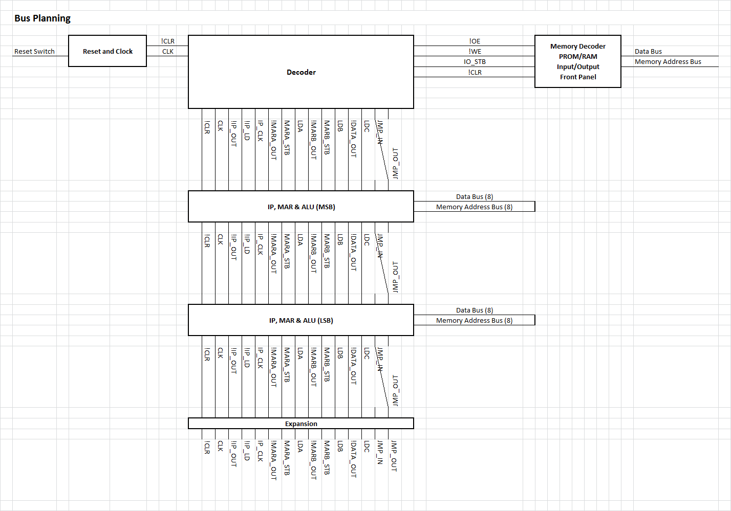
Here my first pass at PCB/bus planning:
You can see that I have:
- I have extracted all the signals I need
- moved the clock and reset logic off the decoder board as I may want to use a different clock
- I have reworked the remaining boards so they can be stacked (a 64 bit CPU?)
- I have not actually designed the Front Panel etc., but have made provision.
Here is the updated schematic with provision for expansion:
Well I can say that it is not often a project get simpler as you progress!
Working
I swapped back to 74LS374s were I could and got the 74LS373s working (just!). I am really pushing my luck with TinaTI! I have got the simulation to execute the infinite loop which pretty well says I got it. The address bus and to a lesser extent the data bus is a glitch mess. I will have to analysis the decoder signals more closely, to find out why. It may just be TinaTI warming me it is close to falling over again. Here is the latest schematic:

I have swapped out the schmitt trigger relaxation oscillator for a gated crystal oscillator and the three 74LS74 D-Latches for a 74LS161.
The signals look okay with an 8 MHz crystal. The crystal oscillator is a little unusual in using a schmitt trigger for the active component but it works well.
I have swapped the strobe signals back to clock signals.
Some tweaks with the ALU carry in and carry out.
16 Bit RISC
I have great expectations for this CPU so I will go to 16 bit up front (two 8 bit stacks).
I need to make up the PROM/RAM/IO board and work out how I am going to interface to the system. I want to do more with this CPU than a Front Panel is reasonable for but have not worked it out yet. Still I think I am ready to get the first set of boards made.
Direct Memory Access
I am not using a Front Panel for this CPU but I still need a way to program the system. One options with a monitor program, seem to be:
- serial
- direct keyboard and video
Without a monitor program:
- direct memory access
Direct Memory Access (DMA) requires a Hold and Hold Acknowledge (like the 8080 system). If the machine cycle has a tri-state at the end of the cycle then I could gate off the clock. I can use T8 by making !OE high instead of low. T7 (the cpu has machine cycles T0 to T7) is only used to advance the IP or to set the IP with the C register (all internal operations) so the !OE does not need to be low.
With DMA, for development programming (i.e. debugging) an Arduino can program the system.
Schematic V9
Reworked the decoder for DMA using HOLD and returning !HLDA (hold acknowledge). The the CPU stop in T7 and the data and address bus go tri-state. The control signals all go high (multiplexing these will have to be done at the memory decoder).
I had to revert back to the old memory write logic (again the write logic will have to be modified at the memory decoder).
So here it is:
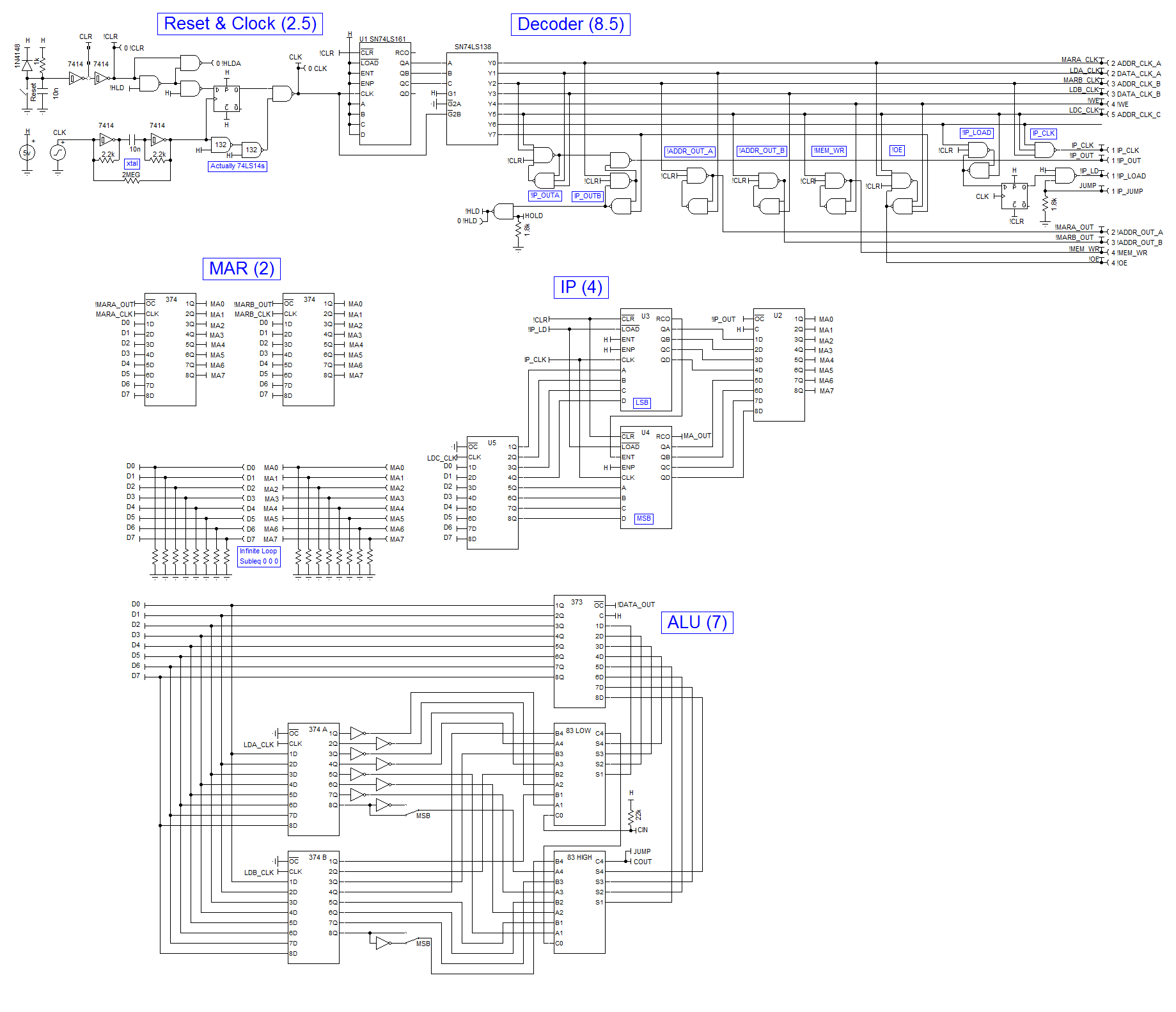
Here are the HOLD signals:
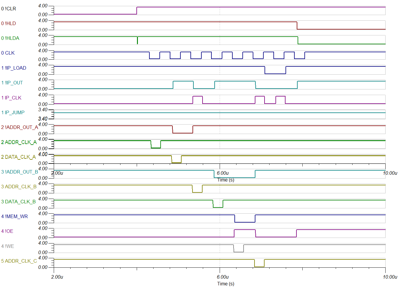
There is a glitch in the !HLDA from the !CLR signal but it is not material.
Back to a simplified 8 bit version
I was running around in circles so I gone back to the simplified 8 bit version. Being 8 bit a Front Panel will be fine (i.e. programs will not be very long). Here is the final 8 bit version that is ready for prototyping:
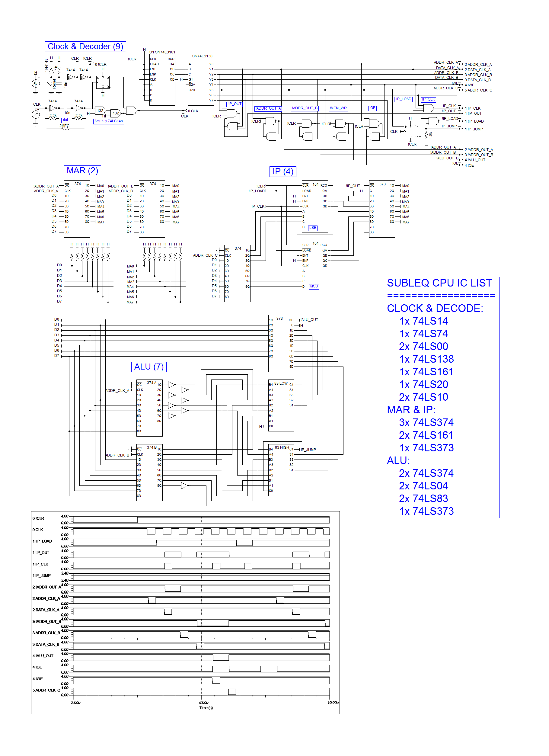
It still does not work in the TinaTI simulator properly but the timing signals look good and I can't find fault in the MAR, IP or ALU.
Now I remember, TinaTI has a limited network depth search. I ran into this problem before. I suspect that the Decoder is more complex than before thus the 74LS373 that used to work before no longer works.
Front Panel
Here is a basic Front Panel added to the schematic:
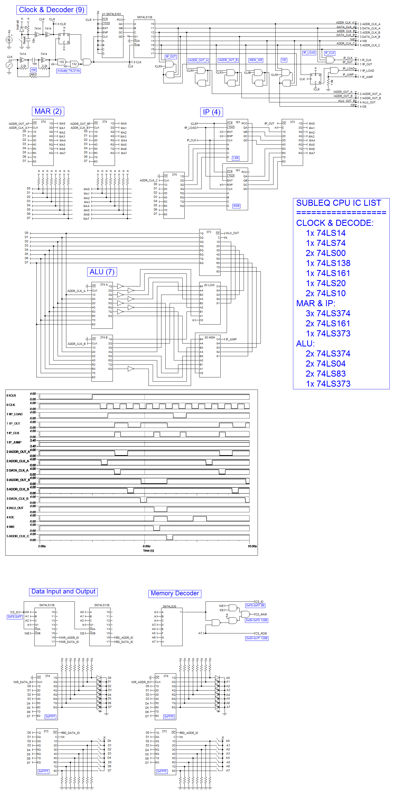
The Front Panel's RAM decoder includes the !WE fix to limit memory conflicts. Unfortunately, the IO write will not work with the SUBLEQ write cycle so will need to be modified. This design assumes momentary contact switches but I will have to use toggle/slide switches as PROM memory space is a super premium.
Opcode SUBLEQ
I want to rework the Decoder to delay the ALU write (to the B address) to after reading the C address so that I have the option to use the high bits of the address space for opcodes. Obviously not for the 8 bit version of the SUBLEQ CPU.
Reworking the CPU
Decoder
- I reworked Decoder, rearranged to fetch order so that "C" is fetched before the ALU result is deposited into "B". This allows the CPU to check the high order bits of the jump address (i.e. C address). For fun I linked the MSB of "C" to the HOLD signal and yes it stopped the CPU (with no way of resting it!). The real reason for this is so I can use the high order bits of the jump address as opcodes (for the 16 bit version of the CPU). The CPU really needs a NAND Jump on Zero second ALU.
- I added:
- !EXT_RST - EXTernal ReSeT for the Arduino
- !EXT_OE - EXTernal Output Enable for the Arduino
- !EXT_WE - EXTernal Write Enable for the Arduino
- HOLD - HOLD the CPU and make the Data and Address bus tri-state
- !HLDA - HoLD Acknowledge (the CPU is now waiting
- I moved the clock off board, the Arduino will provide the clock signal.
Input/Output
The easiest way for the CPU to talk to the external world is to parallel read and write to a port. To do this without timing or control signals is possible if one character is used a marker. May as will use \0 or "null" character. The output stream would consists of sequential characters at any speed (within reason). The CPU (when receiving) would detect a change in the character to signal a new character. Easy, but what about duplicate characters. Easy, insert a null between duplicates (but ignore the null). But what if I want to send a null, bad luck! Not really, we could use an escape sequence such as '\' as used in C code.
Here is the updated CPU schematic (no IO):
TBC ...
AlanX
 agp.cooper
Discussions
Become a Hackaday.io Member
Create an account to leave a comment. Already have an account? Log In.
Hi Yann,
The more I get into this CPU the more magical it gets!
AlanX
Are you sure? yes | no
I love your magic !
Are you sure? yes | no
Wow it's getting... exciting !
Are you sure? yes | no