 Kārlis
First version of PCB was a failure. I didn't properly consider use of regular think the use of regular shift registers with push-pull outputs for driving rows. Only after the PCB was soldered I understood that pressing two buttons on the keyboard will cause rows to short-circuit. Not wanting to redo everything I tried to come up with a workaround, that resulted in more mistakes.
I tried to reduce the short-circuit current by covering contacts with slightly conductive ink made of glue and graphite. That bumped the resistance to 0.5K-2K . In combination with input scanning being done only a fraction of time that should have solved the excessive current problem. After observing that pressing two buttons in the same column still doesn't work I understood that I have made a voltage divider. There was no way of avoiding to redo the PCB.
This time I decided to order PCB from China instead of etching at home. I was getting mixed results with printing the transparent masks. My laser printer really didn't like the material and printing at copy shops were either too transparent or had lines more than half the time.
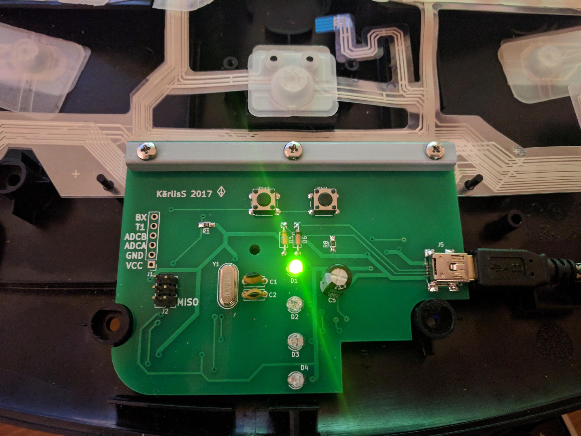
After soldering everything I was ready to start working on firmware. After loading the last test program it was recognized in the USB device list. I was starting to think that I have solved most of the hardware bugs. After starting to experiment with reading keyboard input results didn't look correct. Printing the number of pressed buttons on LEDs showed completely wrong result so I decided to print the whole matrix.
oooooooo
oooooooo
oooooooo
oooooooo
oooooooo
oooooooo
oooooooo
oooooooo
oooooooo
oooooooo
oooooooo
oooooooo
oooooooo
oooooooo
oooooooo
xooooooo
xooooooo
xooooooo
xooooooo
xooooooo
oooooooo
oooooooo
oooooooo
oooooooo
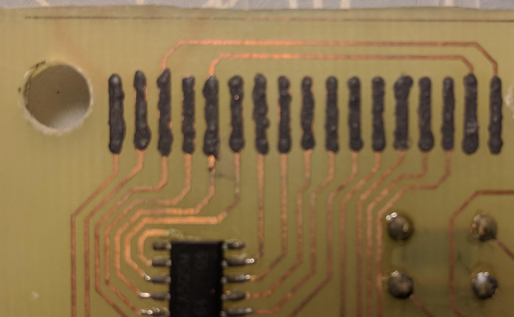
Interesting, pressing a single button resulted in streak. I guess the pull-up resistors built in atmega are too small for capacity of keyboard. That could be solved by adding some delay. It required 10-20uS delay for each row. Having 24 rows that seemed too much. I could switch the inputs to outputs for a cycle charge up the lines faster. Resetting shift register outputs would also take a while. Unfortunately due to lack of outputs for microcontroller and to simplify the layout I had chosen to connect the shift register disable line to ground. It would have been useful to have them now so that I can temporary disable their outputs without flashing the register state. One of the traces to disable pin was going under the chip so I couldn't cut and add a bodge wire. Not wanting to redo everything again I decided to take the risk and leave it as is.
Rewriting the code from
DDRC |= INPUT_MASK;
DDRC &= ~INPUT_MASK;
// to
tmp = DDRC;
DDRC = tmp | INPUT_MASK;
DDRC = tmp;
reduced the time outputs are enabled from 3 cycles to 1 cycle ~ 0.1uS. No magic smoke escaped so far so it's good enough but I will keep in this case other changes to hardware are required.
Discussions
Become a Hackaday.io Member
Create an account to leave a comment. Already have an account? Log In.