Here are some pictures of the various steps of the PCB production. My -not exactly cheap- european fab house sends them per email which shortens nicely the waiting time until the PCBs finally arrive.
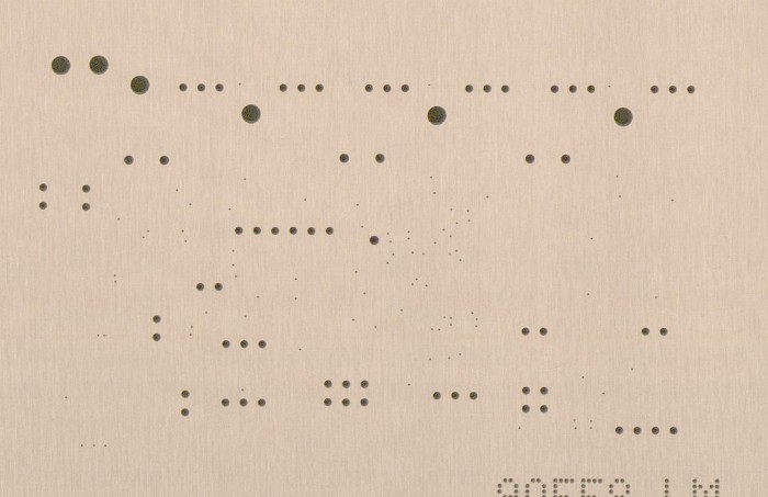
The first step is drilling the holes for THT components and for the vias. It's more than 150 of them!
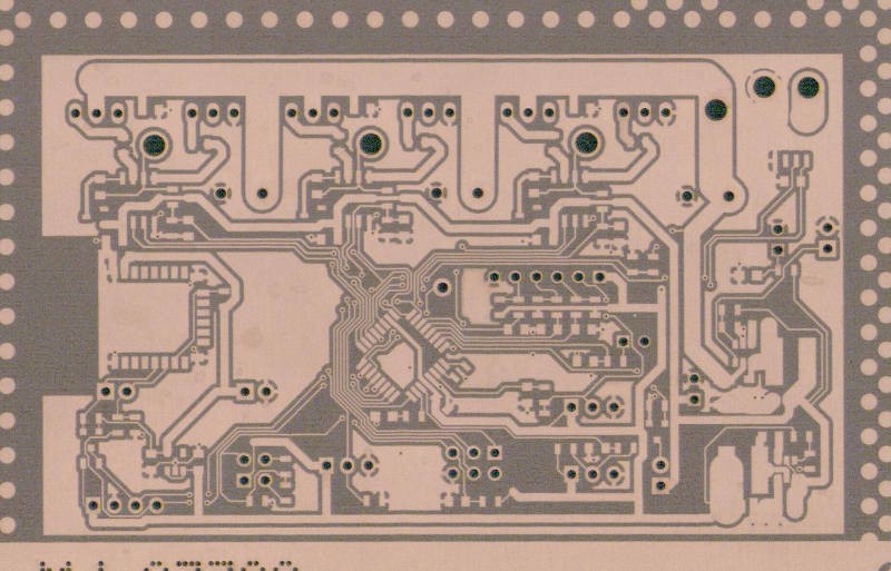
The next step is applying the photo mask and etching. You can already see very well the structure of all the traces.
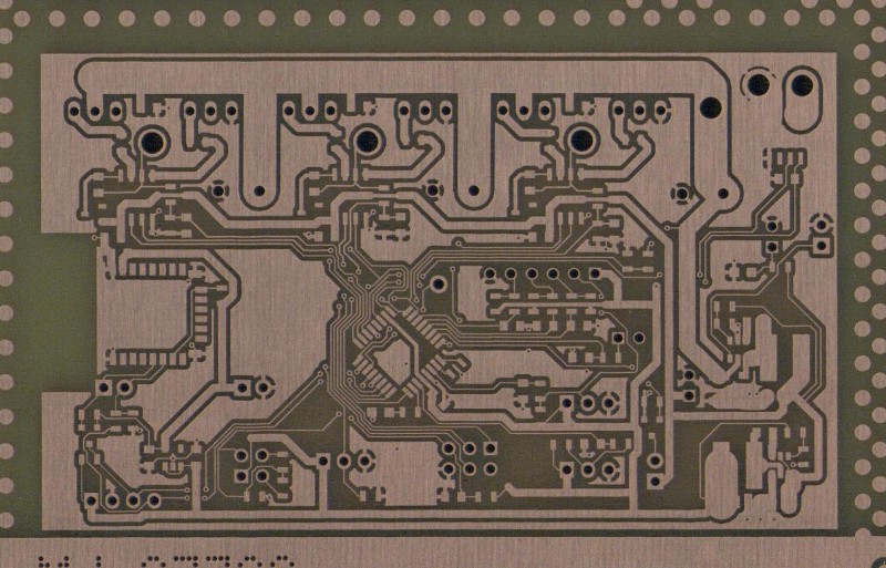
And this is what the board looks like right after the etching:
The final steps are then to apply the solder mask and the silk screen and to finish the pads with ENIG gold plating:
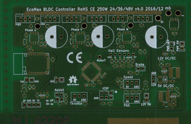
That's it, almost ready. The final steps are cutting and shipping. Pictures of the assembly will follow...
Discussions
Become a Hackaday.io Member
Create an account to leave a comment. Already have an account? Log In.