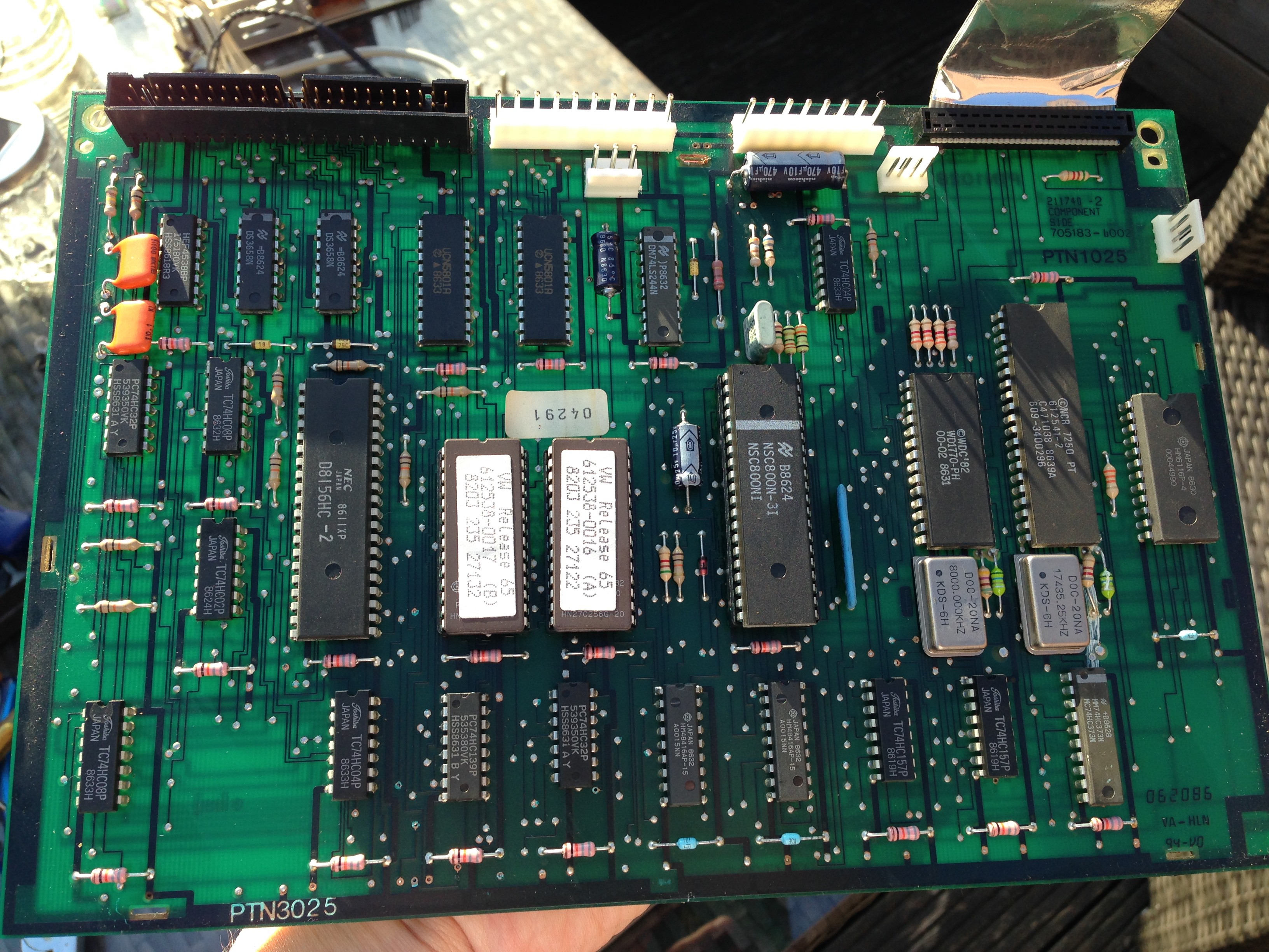
This time to take a look at the main board of the VideoWRITER and take a first guess at how it works. Let's take a closer look at the 7 big chips in the middle row of the board rom left to right. I added the datasheets of all chips (when available) to the project page.

D8156HC-2 - IO controller
This is probably the controller for the printer, judging by its location on the board relatively close to the printer connector in the top left corner of the board. This chip has three I/O ports (two of which are 8-bit and one 6-bit wide), a 14-bit timer and 256 bytes of static RAM. I hope to find out later what each of the ports on the chip is used for and confirm that it's used to control the printer. It's probably also used to communicate with the keyboard. The 8156 uses a combined address and data bus just like the CPU, as we will see in a bit.
HN27C256-20 - 32kb x 8 EPROMs
The next two chips are two 32kb EPROMs that contain the VideoWRITER software. This brings the total to 64kb of ROM, which contradicts the Wikipedia article that states that the system only has 16kb of ROM. This amount of ROM also suggest that there is probably some bank switching going on if the full 64kb is used. That is beacause the CPU , which is going to be a Z80 clone, can only address a maximum of 64kb of memory and there must be some RAM on this thing as well. Spoiler alert: there is 16kb of RAM. So maybe one of the ROMs is being bank switched to select either the upper or lower 16kb of ROM to leave room for the RAM. We will investigate further in a later log...
NSC800N-3I - CPU

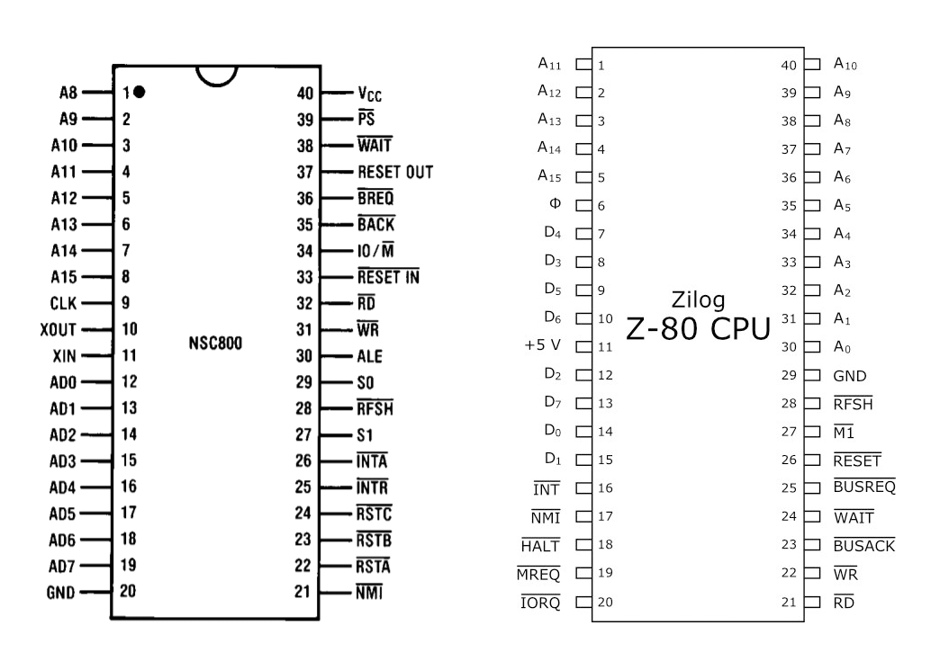
Yes, this is a Z80 clone. However it is only a clone in a sense that it has the same instruction set. The pinout of this chip is completely different of a normal Z80. The pins on the left side of the device are all the address and data lines neatly ordered. The NSC800 has a combined address and data bus. This means that the lower 8-bits of the address bus are also used by the data bus. To select between the two the CPU has an ALE pin that is high when these 8-bits are to be used as the lower 8-bits of the address. The right side of the chip is completely dedicated to control signals like ALE, Read Enable, Write Enable, Memory / IO selection etc. It looks like this CPU is probably going to be harder to work with than a regular Z80, but also this is something we will find out later... From the datasheet we can see that the CPU runs at 2.5MHz, which means that the 5MHz clock from the nearby crystal must be divided by two somewhere.
HM48416AP-15 - 16kbx4 DRAMs
Next we take a little side track to take a look at the two DRAM chips below the CPU. These are two 16kb DRAMs with a 4-bit wide data bus. It makes sense if one of these serves the upper 4-bits of the CPU data bus and the other one servers the lower 4-bit half. So it wouldn't surprise me if I will later find that the address lines of these chips are tied together to form a combined 8-bit data bus.
WD1770-PH - Floppy disk controller
Now this is an interesting chip! We are looking at a Western Digital floppy disk controller. This chip apparently needs only a minimal number of external components to communicate with a floppy disk drive and it can also format floppies using various formats. This short description is not doing it justice, so it's definitely something for a later log.
NCR 7250 PY - Display controller?
For this next one all my searches have come up empty. I don't know yet what it is, but I'm fairly sure we're looking at the display controller here, since it's the only major component still missing.
HM6116-4 - 2kb x 8 SRAM
More RAM? This is probably used by the nearby display controller as its video memory. The display is probably not a bitmap display, but rather character mapped. This means that the RAM will contain the character codes of what is shown on screen and that the display controller maps these codes into a pattern to show on screen using its internal font bitmap. The size of 2kb seems a bit small though, since that would only be enough for a text display of 80x25 characters, while the display seems wider and this also leaves no room for character attributes like bold, underline etc. I could be mistaken though.
Alright. All this leaves enough room for thought and further investigation. For next time I will do some poking around with the multimeter to see if I can work out how the ROM and RAM tie into the CPU and whether the ROM is actually being bank switched.
 Maarten Janssen
Discussions
Become a Hackaday.io Member
Create an account to leave a comment. Already have an account? Log In.