Schematic Debug
I don't have very good tools to test my schematics but Tina can be coerced into something and something is better than nothing. Most the errors I find error are label errors but some of the Tina models are also wrong.
Spend the day testing the CPU. Found lots of schematic error (mostly labels but also swapped internal bus lines). Not surprisingly you cannot read and write at the same time to the same register unless it has been designed for it (i.e. the Data Bus and the ALU). But the ALU only works because the gates between the input and output buffers delay the propagation just enough. But still the 74LS374 are edge triggered so it may be a Tina model problem.
I have changed the ALU to ADD and NAND as CPU internals are not seen on the external bus (i.e. no advantage to working with signed integers inside the CPU).
Adding More Register
Does not seem to be any point not fully populating the registers. No real saving leaving them out. This CPU does not have enough registers (or ROM) to model an Intel 8080 nor enough ROM to decode all the instructions (a 12 bit version might but a 16 bit version certainly could).
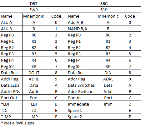
Updated OpCodes
From the opcode table you can see I have packed a lot in, but I have resisted the temptation to add 16 bit support (next time):
The Plan
The plan at the moment is to code the front panel interface directly in the CPU micro-code and to model Subleq as the first CPU model. This allows me to stay with 8 bit with Subleq. Something that I could not do with a straight Subleq CPU.
Vero Board
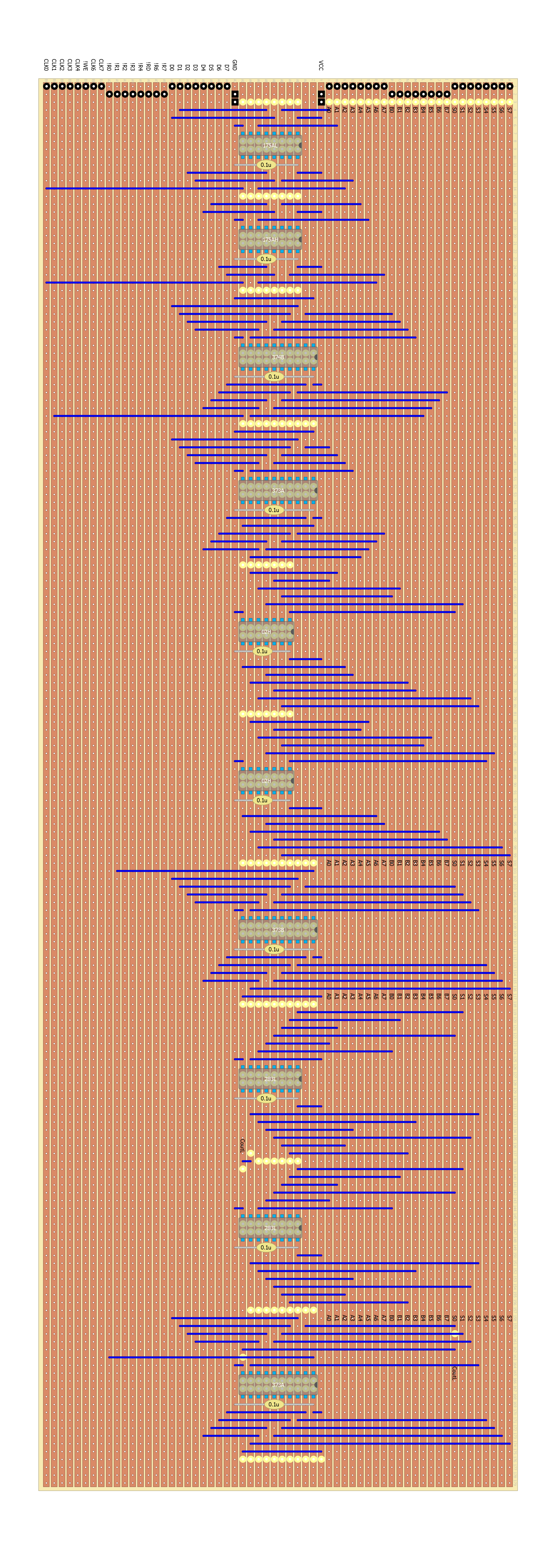
I have knocked up the ALU on a Vero Board. But this is expensive and I will need at least two more boards. The big advantages with Vero Board is that mistakes can be fixed. The down side is a board this size would take a full day to make and it is very tedious:
EasyEDA PCB
EasyEDA is not too hard but one error and the board is useless. That was the problem with the 4BitCPU. But in this case the decoder is much simpler and you do get better at designing PCBs each time you try. I seem to have talked myself into a PCB again!
More Schematic Errors
Spent the day entering the schematic into EasyEDA. Saw that the PC clock was the wrong phase I had inverted the signal. Here is the fixed clock simulation:
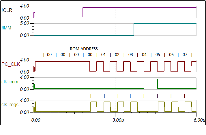
It looks right to me.
Micro-Code ROM
I am using a two 74S571 PROM which are 4 bit and 512 words each but only 256 words are accessible with an 8 bit bus, unless I use a page register (perhaps later). I will use a 6116 SRAM for memory but I am resisting the temptation to add a high address for the time being. So only 256 words are accessible. Here is the current EasyEDA schematic:
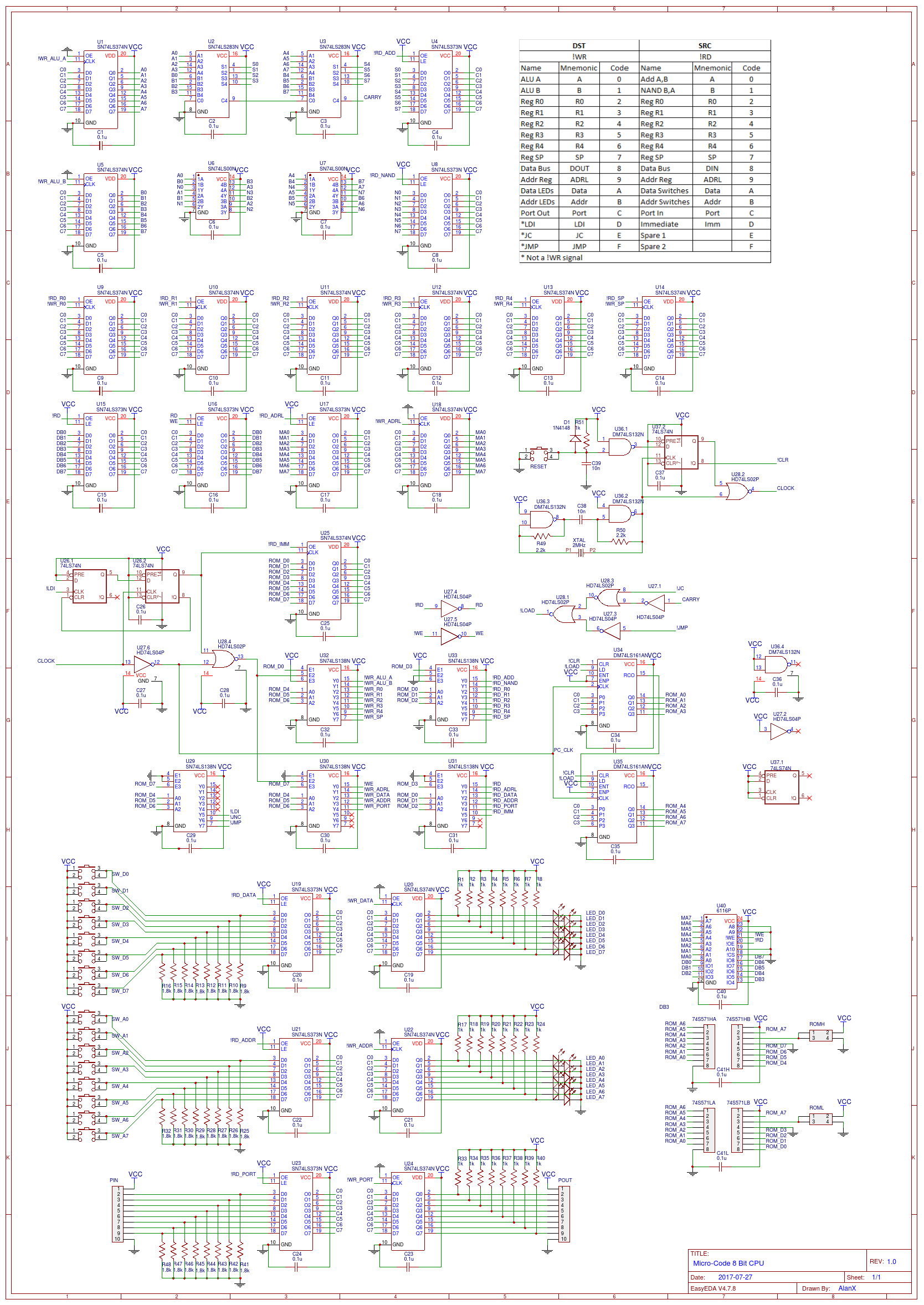
Its is pretty big so I want to spend a day or two checking it.
It is pretty clear I will have to split this schematic into three boards:
- Registers
- PC and control
- IO and memory
Monitor Code
Spent some time coding a monitor program. The code is very similar to the Weird CPU.
I also wrote an interpreter for the code but it is a bit tricky. If I print the registers for each step, the delay routine spits out ~25,000 lines alone. Really I need to use an Arduino and a front panel but I don't have a front panel.
Anyway here is the monitor code:
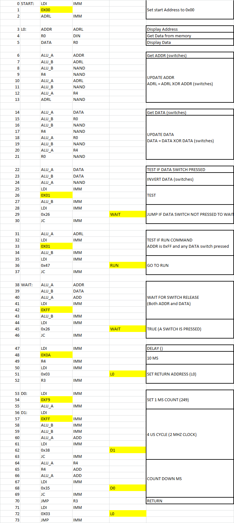
Looking at the code after I have loaded it I seem to have forgotten to save the updated data back to memory!
AlanX
 agp.cooper
Discussions
Become a Hackaday.io Member
Create an account to leave a comment. Already have an account? Log In.