Vector Network Analyzer
open hardware 2 GHz to 13 GHz two-port vector network analyzer
open hardware 2 GHz to 13 GHz two-port vector network analyzer
To make the experience fit your profile, pick a username and tell us what interests you.
We found and based on your interests.
With two port measurements on network analyzer somewhat working, I created a small microstrip test board to evaluate a SMA connector footprint and transition to microstrip.
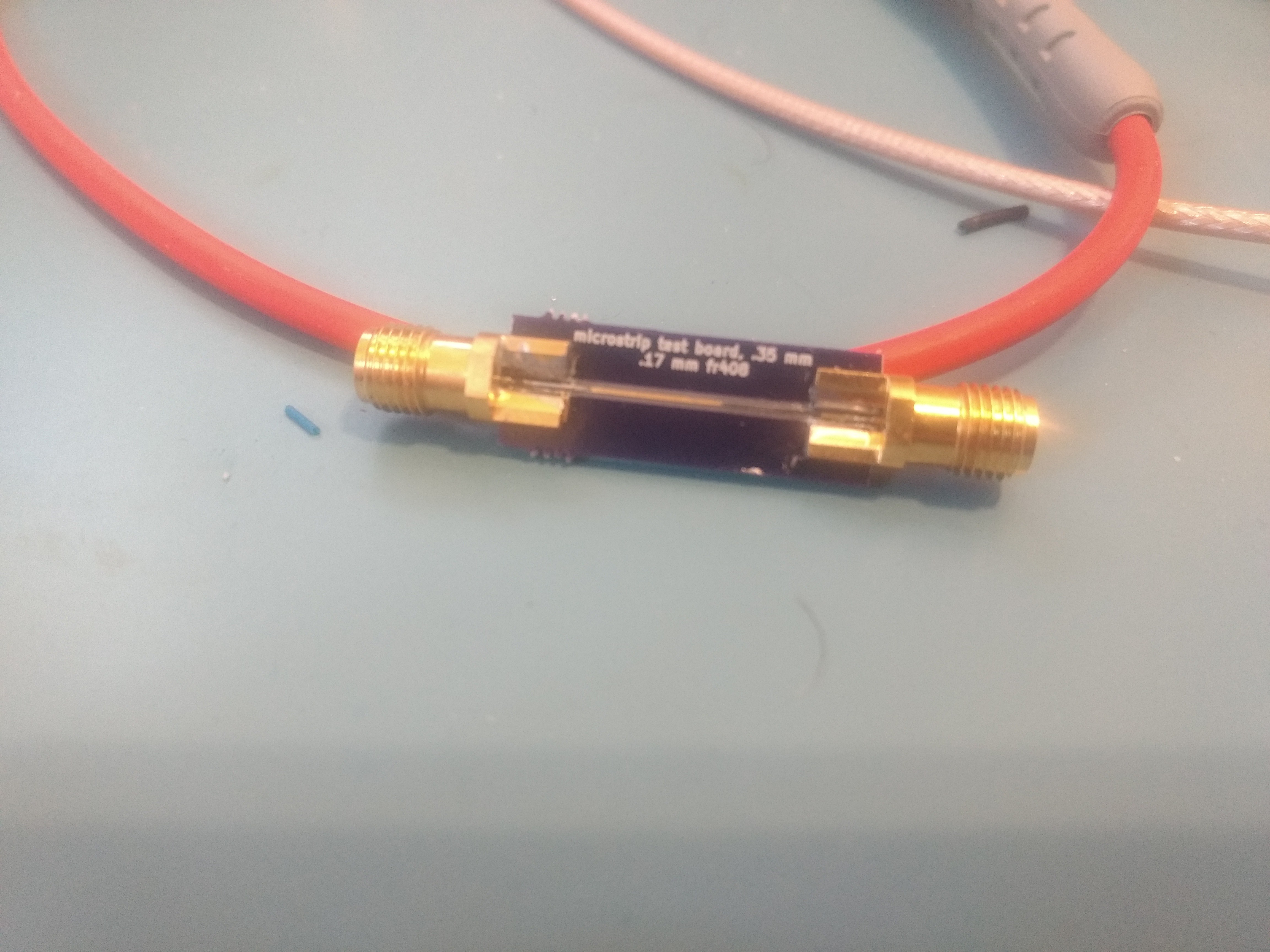
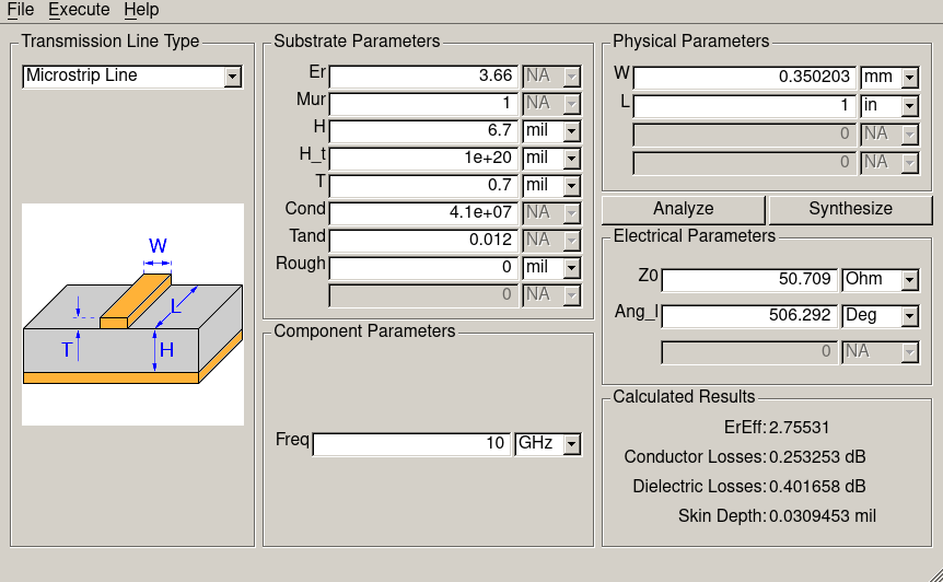
Here are (possibly incorrect) measurements of the test board from the network analyzer prototype: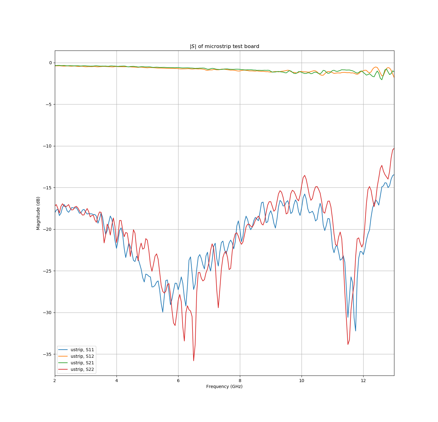 It looks.. okay. S21 at 10 GHz is about -1.2 dB, and S11/S22 are generally below -15 dB out to about 12 GHz. Running the OSH Park 4 layer stackup through the qucs line calculation tool, I would expect about .65 dB of attenuation through the microstrip. If that is correct, it leaves about .3 dB through each of the connectors.
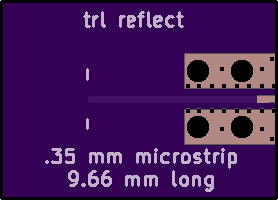
S11 and S22 aren't as low as I was hoping, but I'm not sure if that is from the microstrip or from the connector footprint. To separate out the microstrip testing from the connector footprint testing, I'm making up some TRL (thru reflect line) calibration test boards to extend the calibration plane of the network analyzer past the connectors. TRL calibration will also remove my dependence on an uncertain SLOT cal kit and make it easier to investigate if the ripple in my measurements is from incorrectly defined calibration standards or some other issue with the VNA.
I made a few modifications to the SMA connector footprint compared to the earlier test board to make assembly easier. The clearance between the microstrip and the ground pads is increased a little, and I added back in the soldermask to stop solder from wicking down the microstrip.
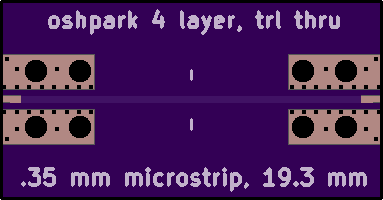
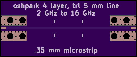

I'll post an update on the status of the TRL calibration in a few weeks once the boards arrive.
The final module to test of the network analyzer is the four channel demodulator.
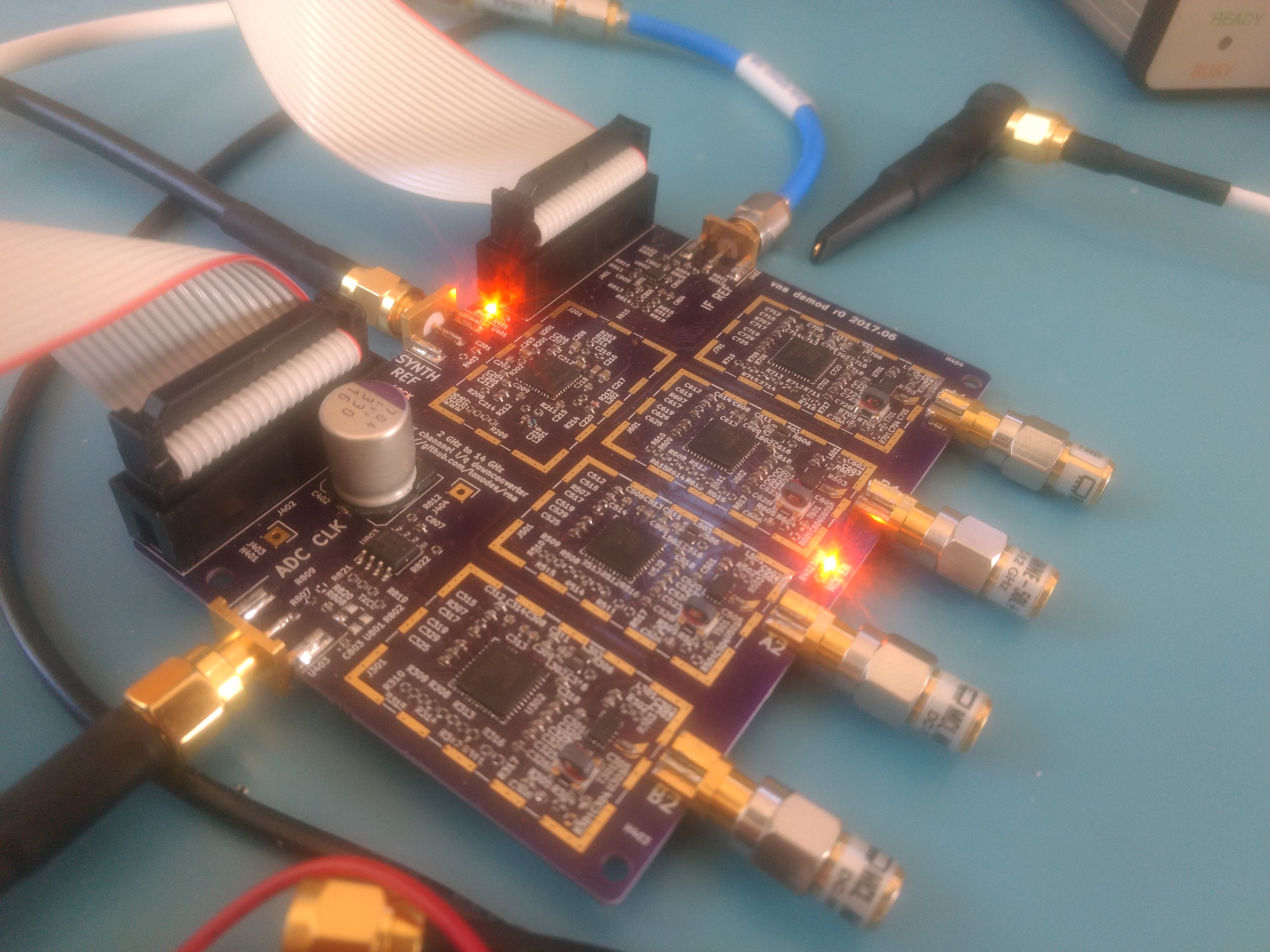
This board mixes down four microwave channels to a 48.25 MHz IF frequency then simultaneously samples them.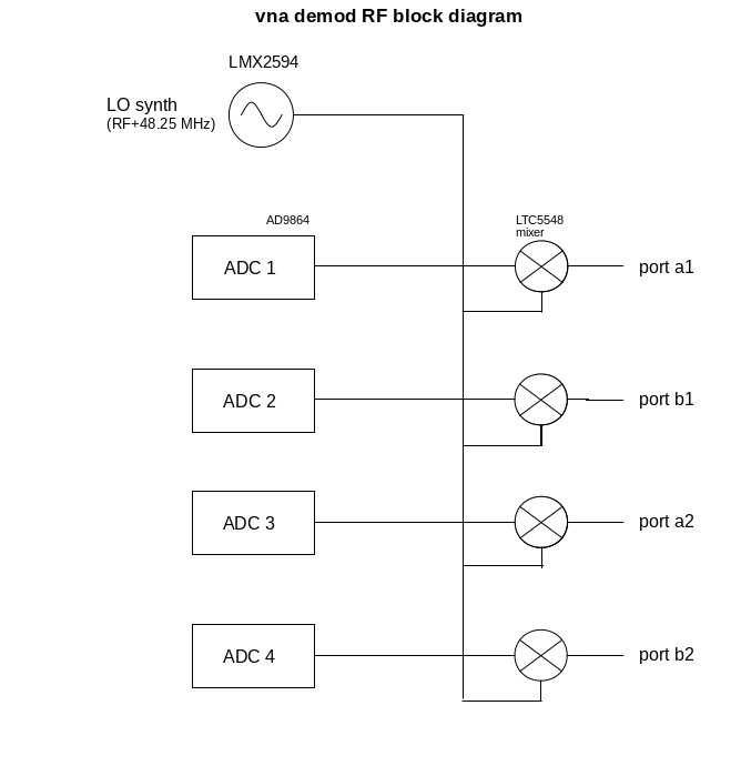
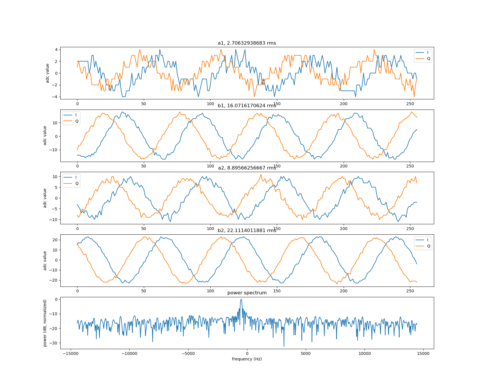
Other than a bad solder joint on one of the mixers, bring-up on this module was uneventful. However, I uncovered leakage problems with the RF synthesizer board while testing this board. There is still a signal at the ADCs even when the synthesizer outputs and demodulator inputs are terminated - to the extent where |S21| and |S12| approaches -50 dB by 13 GHz with both ports terminated. To illustrate this, here are raw samples off the demodulator at 13 GHz:
And here are samples at 2 GHz showing little coupled signal:
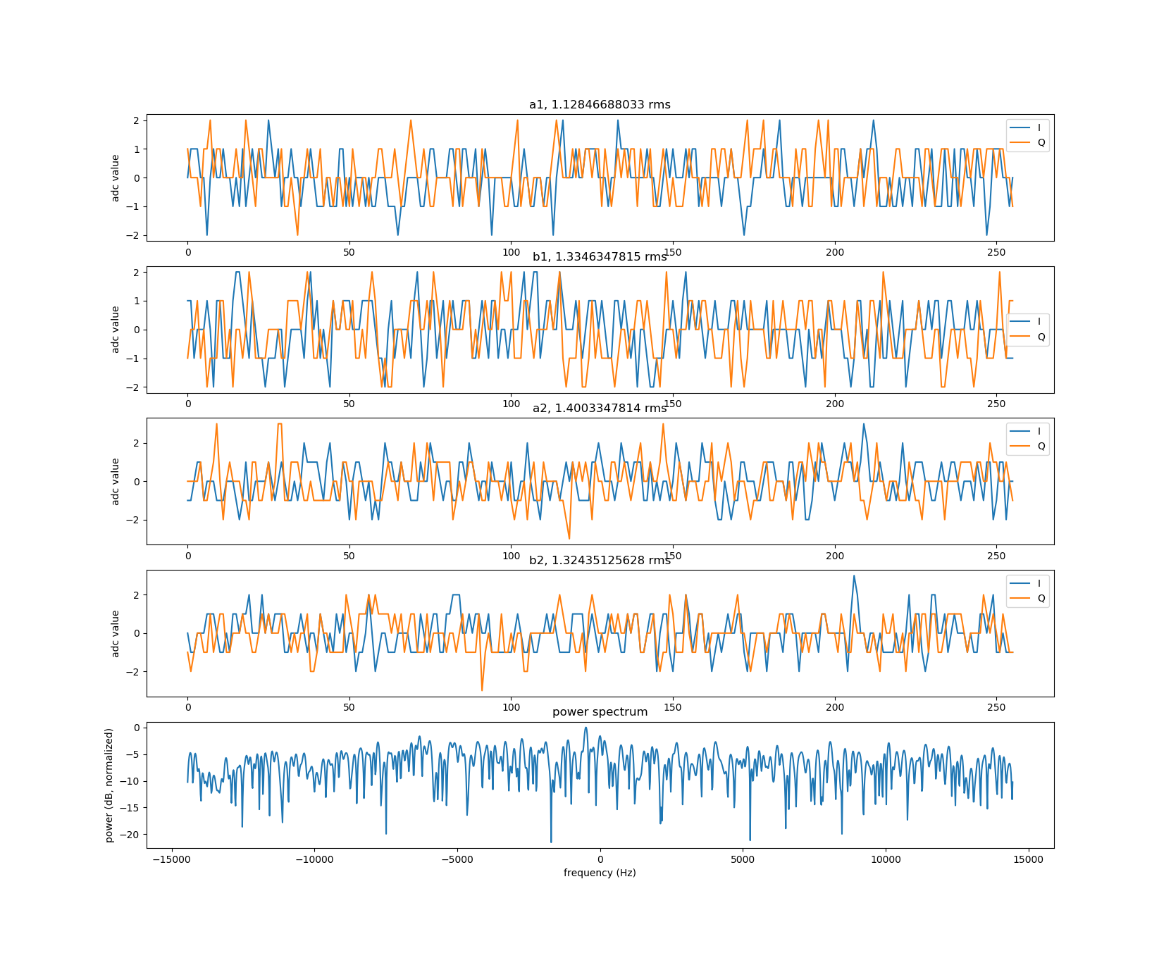
This signal goes away when the synthesizer is powered off, so I suspect this is a problem with the synthesizer signal coupling into the demodulator board. Populating the shields on the synthesizer board didn't improve isolation much so I suspect this is at least partly due to conducted emissions through the data/power cable.
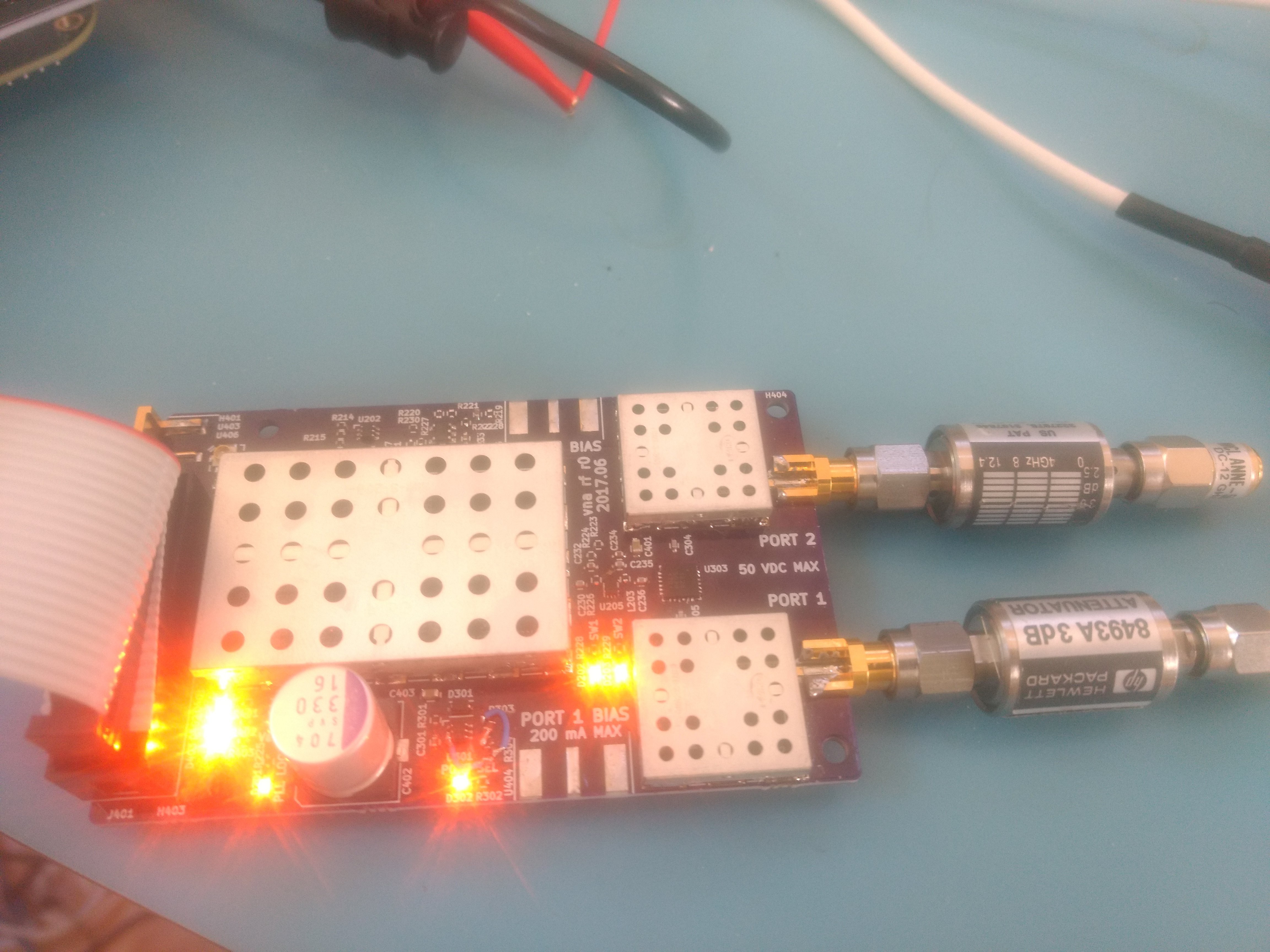
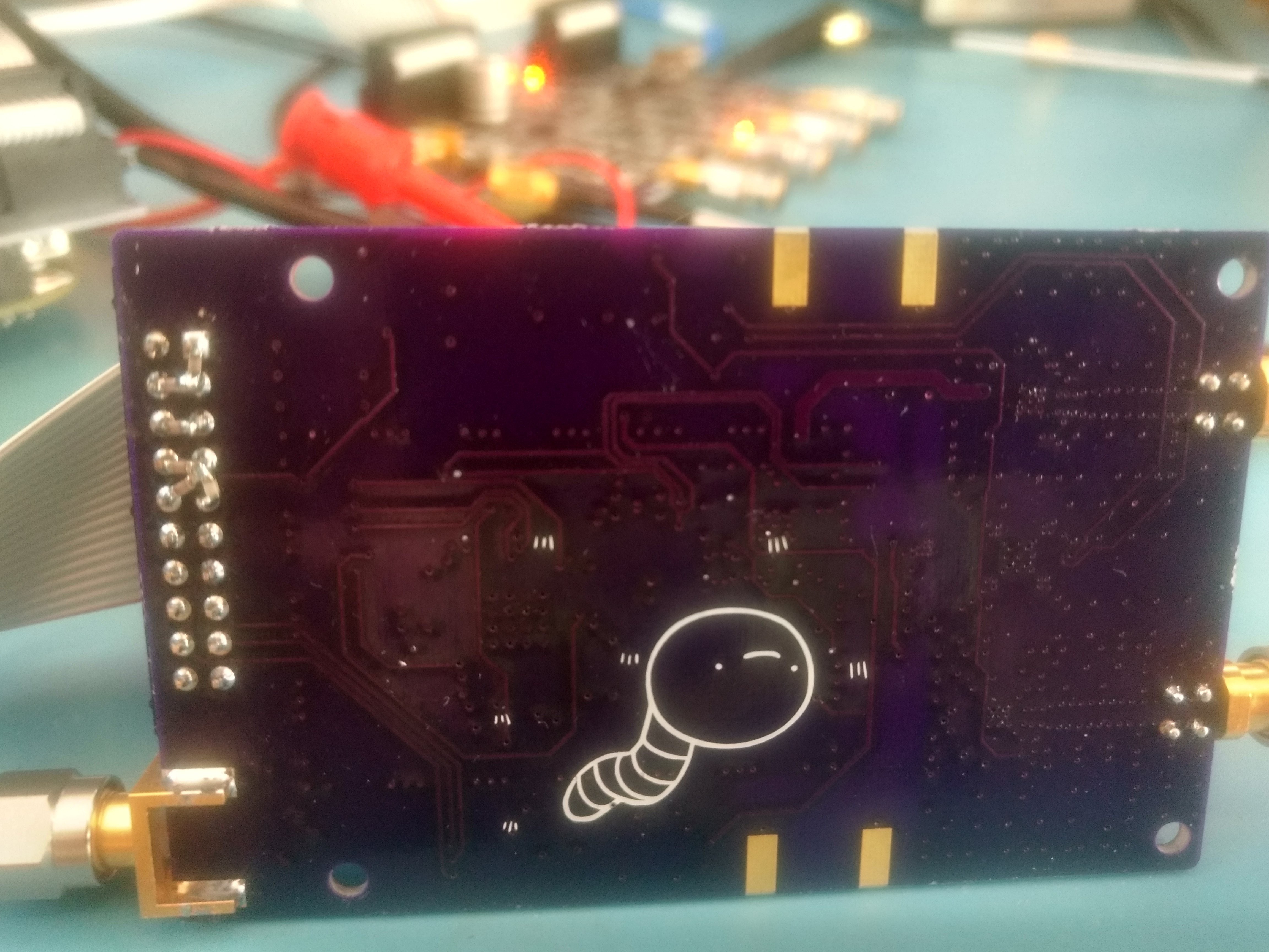
Decoupling the data lines off the synthesizer board that had easy access to ground with 10 pF capacitors improved isolation by about 6 dB. I'll need to be more creative to find a way to bodge on capacitors for the remaining data lines..
Even with the isolation issues, the VNA produces plausible looking measurements. The measurements have more ripple than with the previous iteration of my VNA. I suspect this is at least partly due to inadequate calibration standards. Earlier I was defining my calibration standards from measurements taken with an Agilent E5701C calibrated with a 9 GHz ecal. Since those measurements only went up to 9 GHz, now I'm assuming the open, short, and load have ideal reflection coefficients after some electrical length. I need to look at the E5701C measurements of my calibration kit and see if I can extrapolate a better approximation of the standards.
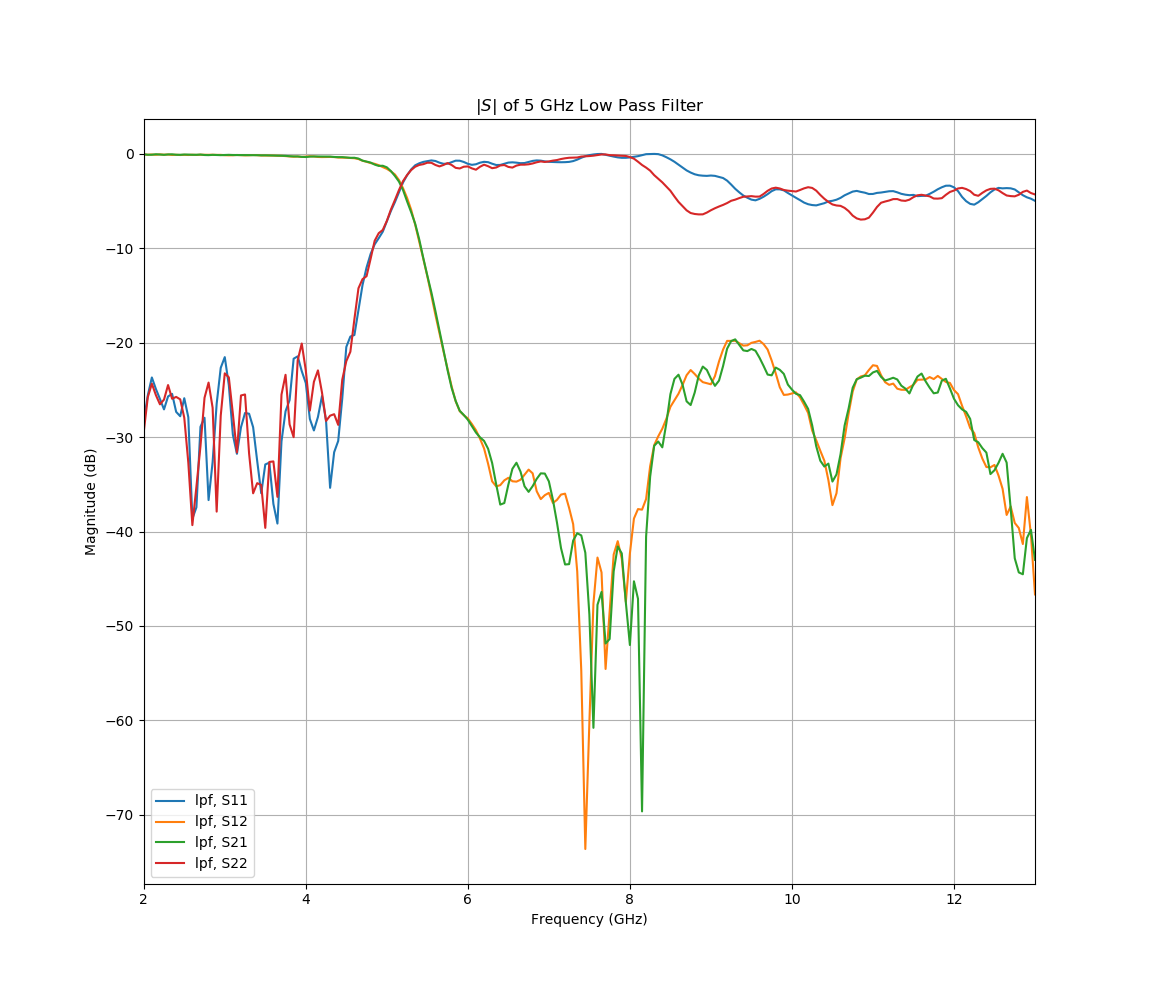
Here is a 5 GHz stepped impedance low pass filter:
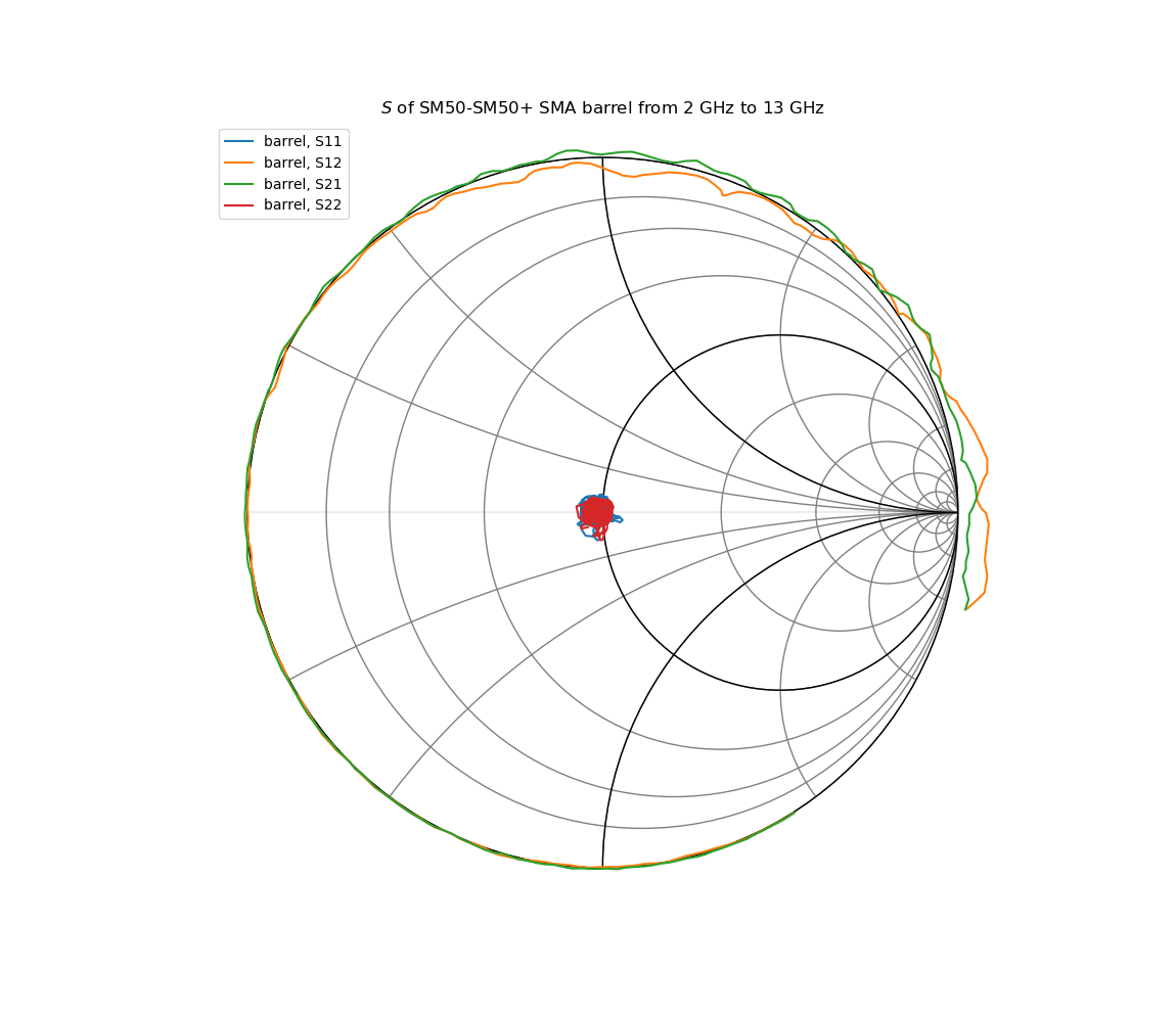
Phase measurements on a SMA barrel look plausible:
There is some probably non-physical ripple in the return loss. I suspect at least some of this is from reflections into the demodulator board. I ordered some used 3 dB attenuators off eBay to try out ... resistive matching, maybe they will improve measurements a little.
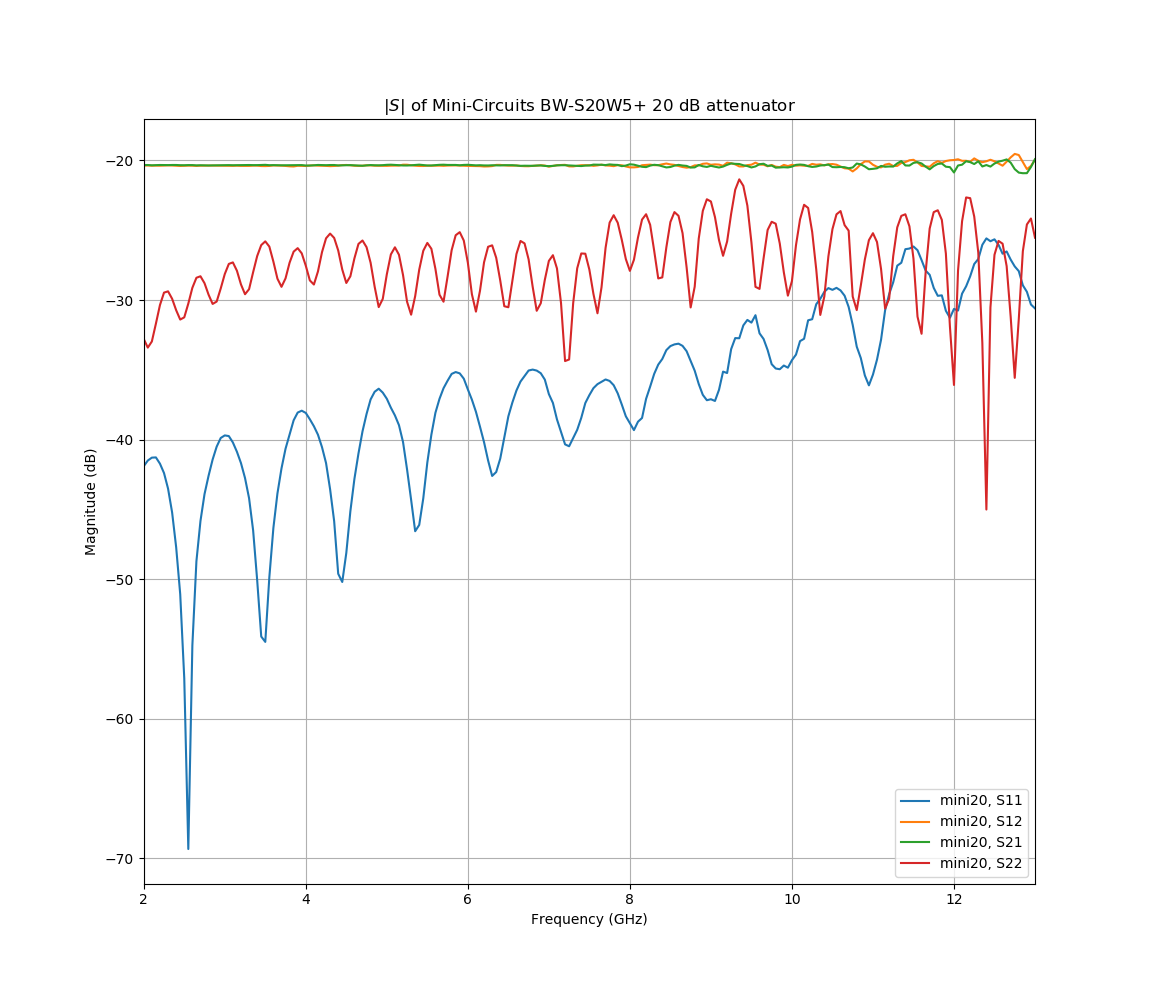
The network analyzer produces reasonable looking measurements, but I still have work to do on improving calibration and isolation.
The network analyzer is controlled with a BeagleBone "cape". This board provides power management, reference clock synthesis, and routes IO pins on the BeagleBone to headers for the other modules.
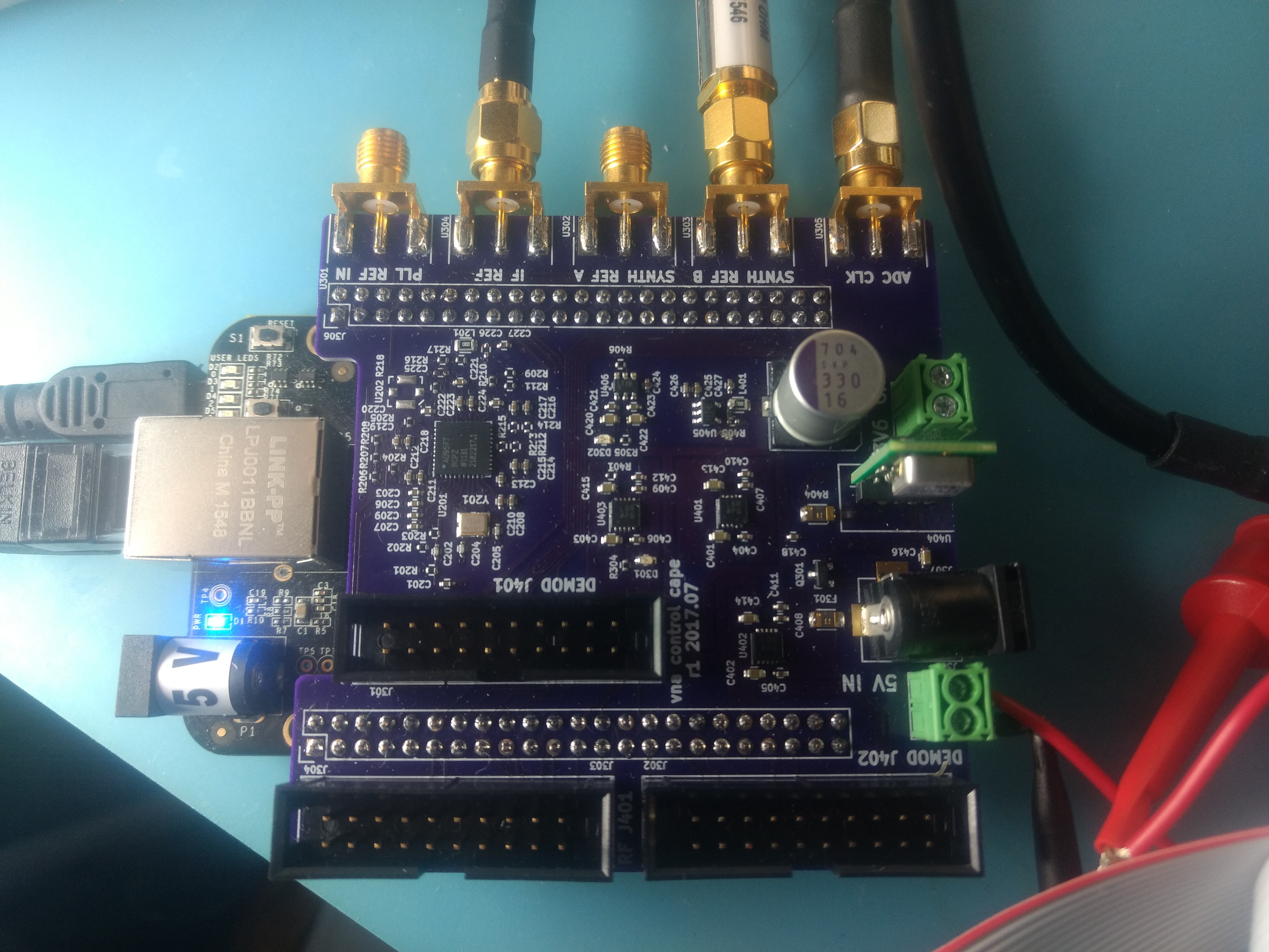
Clocks synthesis is done with an AD9577. Control of this chip is surprisingly simple over I2C, my software (almost) worked on the first try. This chip has two VCOs and PLLs, each with two differential output channels. I'm referencing all the clocks in the signal chain to a single crystal to reduce relative drift between all the clocks. An earlier revision of the VNA had separate oscillators for the RF and LO synthesizers, which made the resulting IF squirrely. The decimation filters on the ADC aren't particularly flat, so keeping the IF frequency stable is important for the stability of measurements.
An on-board The 26 MHz crystal (or an external reference clock) is fed to the PLL/VCO which synthesizes two 85 MHz synthesizer reference signals and a 48 MHz IF-LO tone. The 26 MHz clock is also buffered to provide an ADC reference clock.
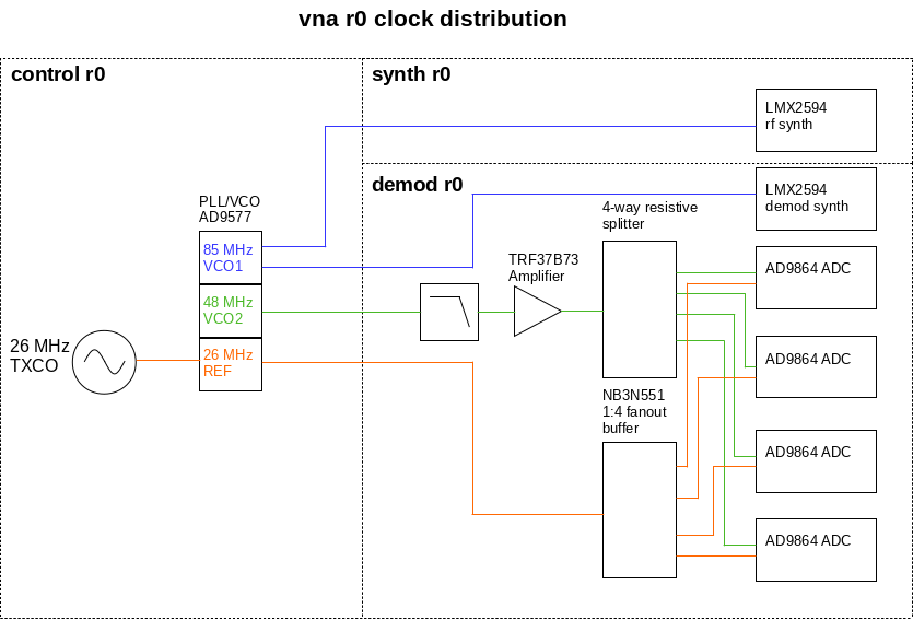
A single 5V input powers the network analyzer. The 5V input rail switched directly to the variable gain amplifier on the RF synthesizer board, and taken by switching regulators to create -5 V and 3.6 V rails. Each of the modules has an independent switchable 3.3 V rail regulated with an LDO off the 3.6 V supply. Other than mixing up pull-up/pull-down on enable/power-down lines, all of the power distribution worked without any issues.

Bring-up of the power distribution and clock synthesis were uneventful. The only debugging excitement on the control cape arose from a short between signal lines, possibly due mask containment issue during manufacturing. When testing the ADCs on the demodulator boards I noticed that the values of the sampled signal looked .. strange. Probing with an oscilloscope revealed that two of the ADCs were apparently sending trinary "trits". I suspected that was the result of a battle between output drivers, so I powered down the VNA and located a short on the control PCB with a multimeter.
I didn't see any obvious shorts and the bridge was measurable on an unpopulated board, so I fired up my thermal camera. The short was approximately localized by running a current limited power supply down the two signal lines on an unpopulated board. This heated up the traces and illuminated the path of the current.
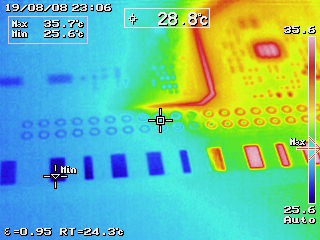
The thermal image narrowed down the short location to the right side of the board near U406.
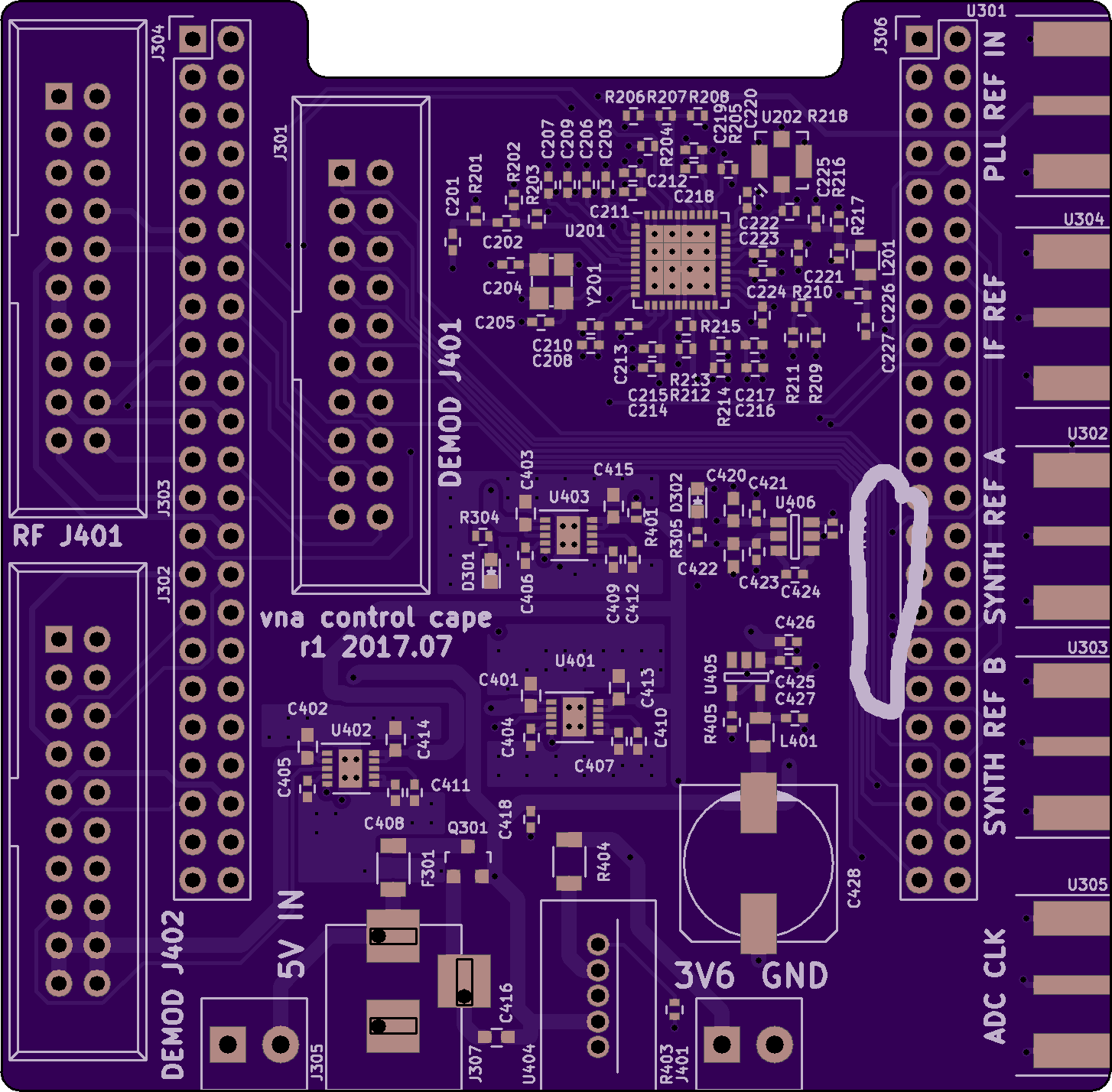
Even knowing where to look I still couldn't spot any bridges so I started hunting with a microscope.
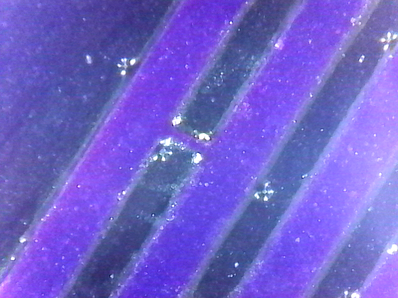 At 250x magnification I spotted a 1 mil thick bridge between the two signal lines. Once I knew exactly where to look I backed off on the magnification:
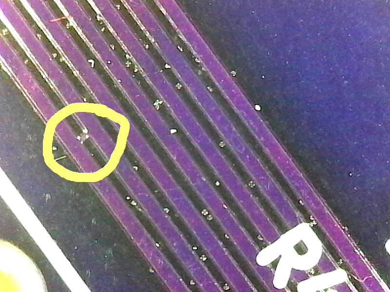
I cut the bridge with a knife then verified that short was eliminated with a multimeter (and checked that none of the other closely packed signal lines had bridges with adjacent traces).
I sent the PCB vendor pictures of the bridge and asked them to isolate where in the process the error was introduced so I could hopefully avoid this in the future. They suspected that it was a mask contamination issue at the fab and immediately issued a full refund for the PCBs without me requesting one. (The short appeared between traces that were right at minimum 5 mils spacing specified by the manufacturer, I'll back off on that a little on future boards if space permits.)
With the copper bridge cut, the VNA control board appears to be fully functional. The next update will describe testing the four channel simultaneous demodulator board.
This weekend I tested the RF synthesizer module for the network analyzer. It is essentially a two port signal generator which will inject a signal into the device under test. The module can spit out an output signal between 400 MHz and 13 GHz with an adjustable power level ranging from around -20 dBm to 10 dBm.
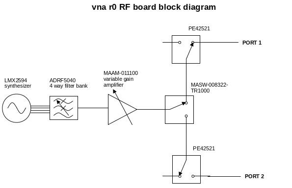
During testing I uncovered many many software bugs (this was my first time using a TI LMX2594) and a few hardware ones. Some of the highlights were that I flipped the polarity of the control signals into the high isolation RF switch (see the blue bodge wires below), soldered a filter in sideways, and messed up the feedback resistors on the amplifier that buffers and inverts the control voltage for the variable RF amplifier.
Here is a picture of the module after the repairs: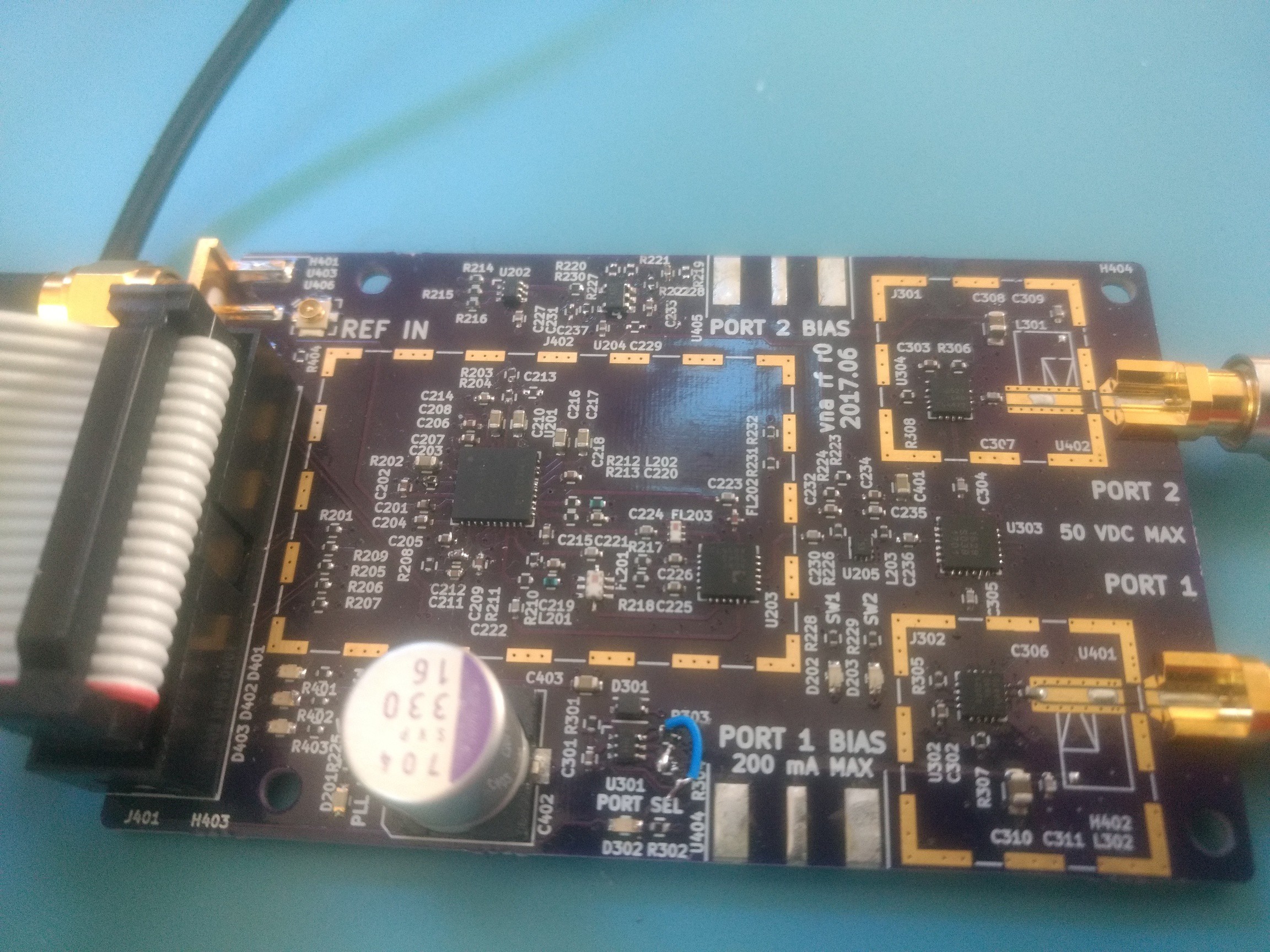
The two output ports can be fed with a DC bias input, this might be helpful for testing active devices like amplifiers. I didn't fully populate this yet because I want to make sure everything else is working before I plop down a pair of fancy $30 conical inductors. The board also has footprints for shielding, but those are also unpopulated until I've finished testing.
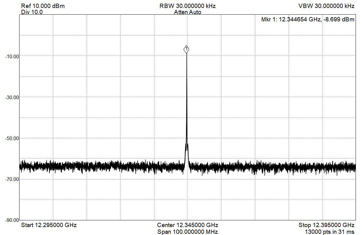
I spot checked a few frequencies on a spectrum analyzer to verify that the signal can work it's way through each path of the filter bank. Here is 12.345 GHz:
Here is a spot check of harmonics at 3.6 GHz. Harmonics will be very frequency and output power dependent, I may need to script up something to sweep this..
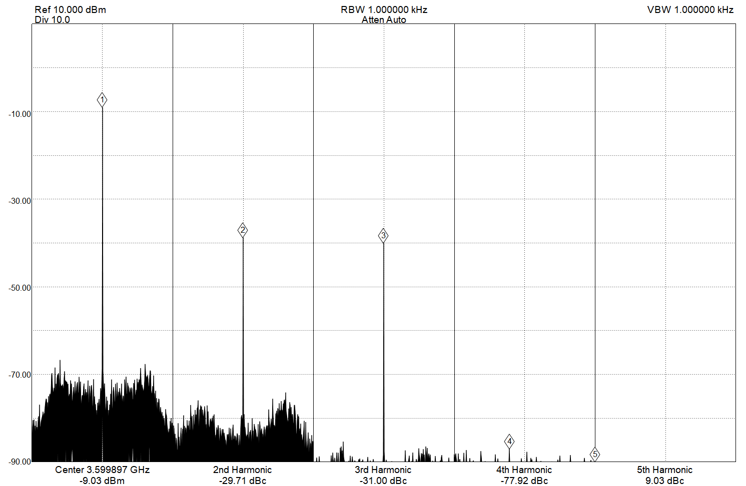
Phase noise isn't great, I still need to dive into the LMX2594 register and PLL loop filter:
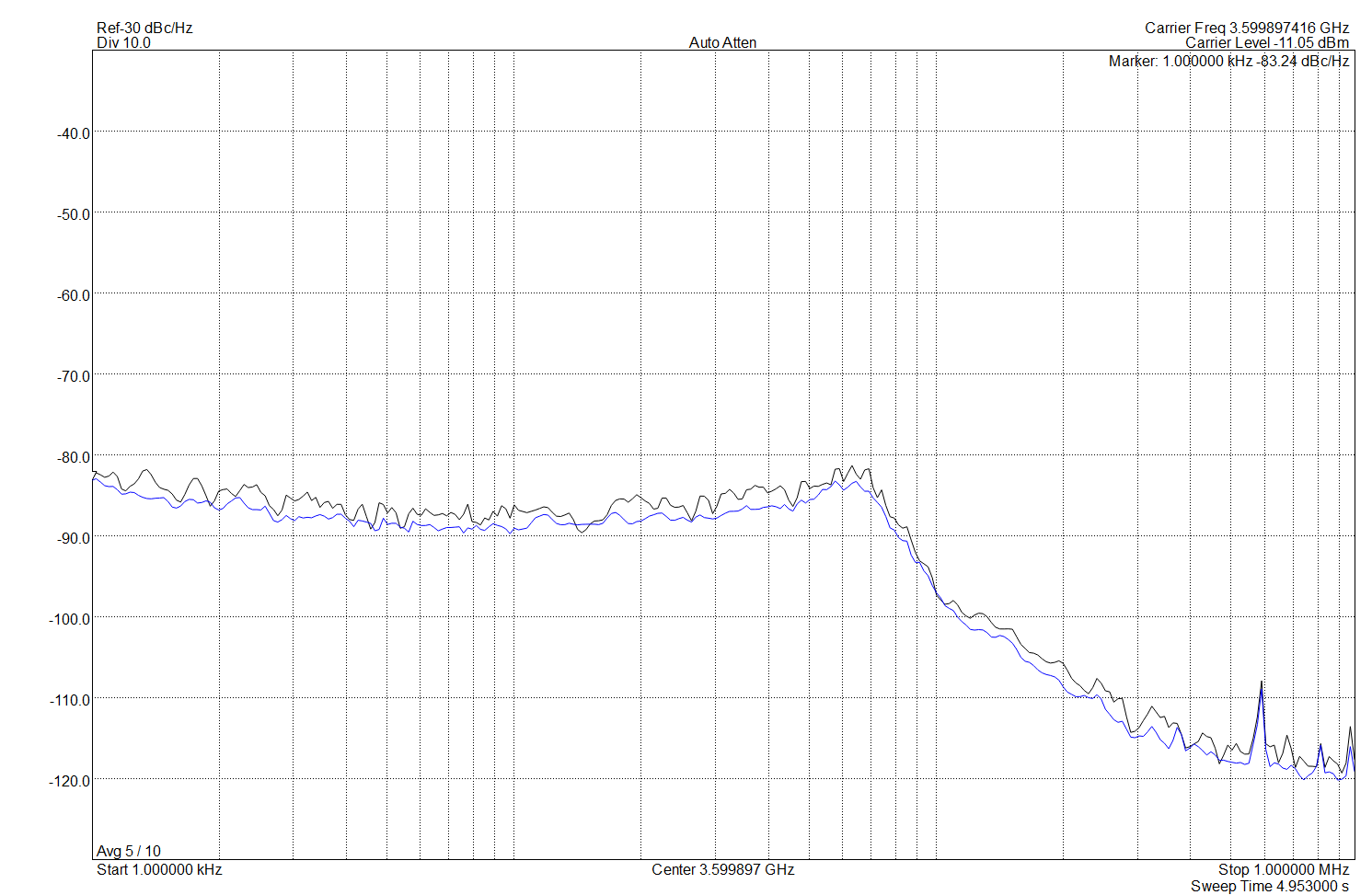
Now that the RF board is mostly working, I'll move on testing the four channel demodulator board. The demodulator board also has a LMX2594 synth, now that I have a working LMX2594 driver testing should go faster.
I'm going public with an open hardware microwave vector network analyzer (VNA) project that I've been developing as a hobby on and off for the past 20 months.
I'm trying to develop a reasonably priced (for a network analyzer..) microwave VNA that could be useful for hobbyist RF/microwave projects. VNAs can be quite expensive (~$3000 for a decades old HP boat anchor useful up to maybe 6 GHz, new ones cost between the price of a car and a house), so I'm building one for my lab.
All project files are hosted on GitHub. Documentation on GitHub currently reflects an earlier 2 GHz to 10 GHz one-port (isolation wasn't good enough to call it two-port..) revision of the project. For some more information on the previous revision, here is a presentation on that stage of the project.
Anyone who wants to try and replicate an open hardware VNA right now might want to look at Henrik Forstén's design. He scooped my project by a few months and has a more cost effective and polished project. My VNA has a similar topology, but I'm throwing more money at the problem in the hopes of achieving better dynamic range and higher frequencies.
I am currently testing the next revision of the VNA hardware. My previous revision lacked isolation and it was quite expensive because it was too modular. (Each microwave RF connection between modules costs about $30 from the two SMA connectors and a SMA cable...)
My current revision is split into just three (down from over a dozen) modules.
I'm currently using ebay-ed directional couplers. I'll look into designing my own once I have a working network analyzer to test them with..
Testing of the BeagleBone cape and RF synthesizer boards is in progress. They don't fry themselves and look like they could work, but I don't recommend that anyone try building them yet. I'll post updates to the log as I finish testing of these modules.
Create an account to leave a comment. Already have an account? Log In.
My suggestion is https://icons8.com/illustrations - exceptionally high vector quality cartoon characters and artwork. All assets are free to use in personal and commercial projects, and also - attribution isn’t required, so enjoy!
If it can run the BeagleBoard.org images, consider using the BeagleBoard Compatible logo to support the non-profit foundation (https://beagleboard.org/logo)
Become a member to follow this project and never miss any updates
 Shane Burrell
 Mark Omo
 P
P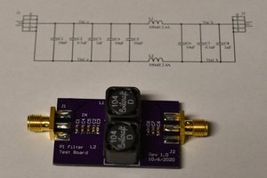
 Bharbour
Quite interesting project. Thumbs up!
Hope to have further continuing details..
Analog Devices introduced ADL 5960 frontend for low cost VNA( up to 20GHz freq.) Oct. 2021, which seems also quite promising.