Timing
Ideally I would like the MC14500B and the MC14500 discrete clone to be compatible so that any circuit I build I can swap one out for the other.
I looked at the timing signals of the MC14500B and I find the WRITE (pulse) signal is probably too slow for modern memory (and even old memory) components. These two reference resorted to shaping the write pulse due to the issue:
- https://github.com/nicolacimmino/PLC-14500
- The Demonstration System from the MC14500B_Handbook.pdf
Although I did look at merging DIN and DOUT of the clone to single DATA signal as per the MC14500B, this is not really a great idea. The separate data paths are better as the DATA signal conflicts for the MC14500B (i.e. two common outputs during the timing cycle) with the muliplexed Input Data signal (if the WRITE signal is used for data multiplexing, which seems to be the way this signal is used). The conflict does not seem to worry the MC14500B but a current limiting resistor in the Input Data multiplexer signal line would seem to be a good idea.
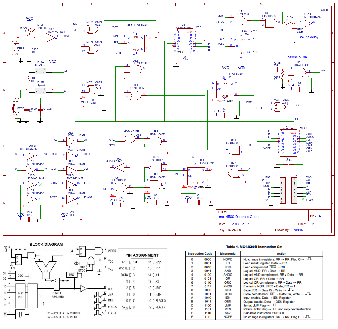
For the clone I have stayed with the full cycle WRITE signal (as opposed to the half cycle WRITE PULSE of the MC14500B) and added a separate /WP signal for the Data Output Addressable Latch.
Here is my schematic of the MC14500 Discrete Clone:

TBC ...
AlanX
 agp.cooper
Discussions
Become a Hackaday.io Member
Create an account to leave a comment. Already have an account? Log In.