Version E of the One Bit CPU
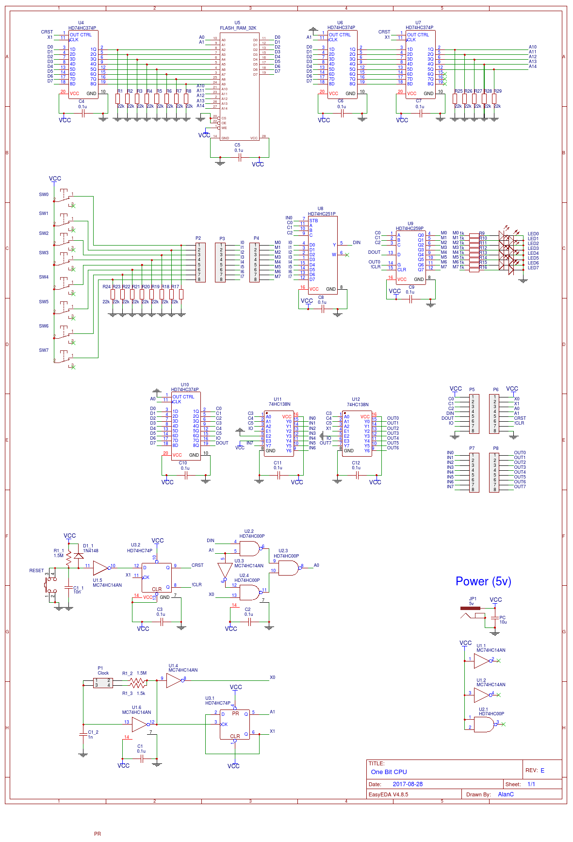
I updated the schematic and the PCB of the One Bit CPU.
- I fixed up the two schematic errors.
- Removed the single step (does not work that well)
- Reworked the clock circuit
- Removed some redundant circuity
Hers is the updated schematic:

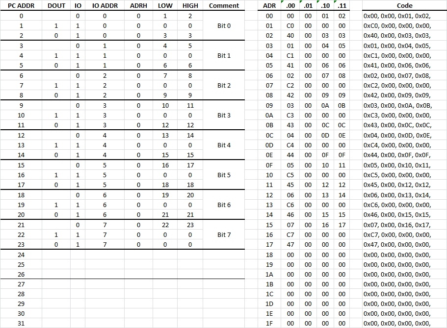
Here is the test program:
Spend a few moments to see that DOUT, IO and IO ADDR are merged into one byte.
- DOUT is ignored for an input (IO=0).
- IO equals 0 for an input and 1 for and output.
- ADDR IO is a 6 bit input or output address.
Th high address (or page) is ADRH.
The low address is either LOW or HIGH depending on the value of DIN (the read value from the selected input).
Each instruction (PC ADDR or ADR) is four bytes, therefore when using a 32k flash ROM it has 8k program space.
You may see that the One Bit CPU is basically a Finite State Machine (FSM).
Demo Program
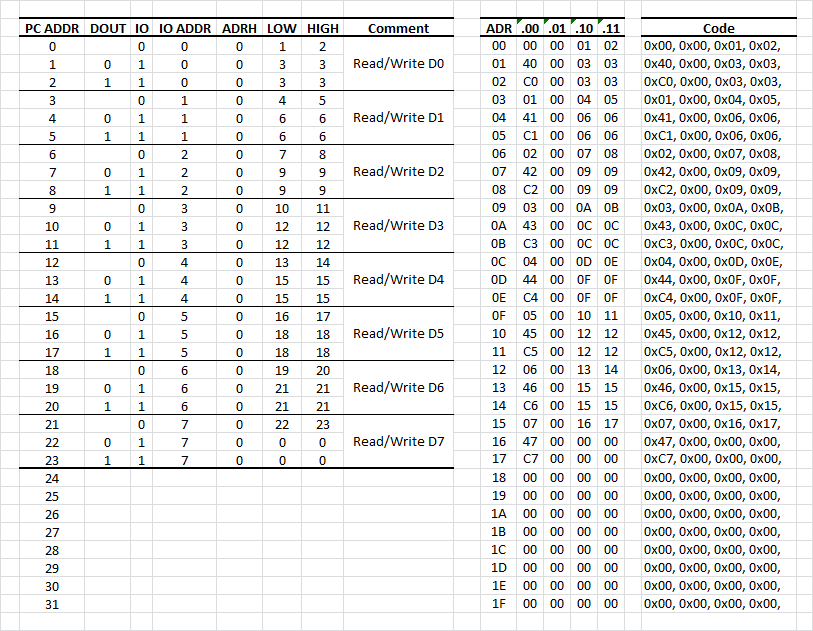
A demo program needs to do something visual. So I coded a binary counter:

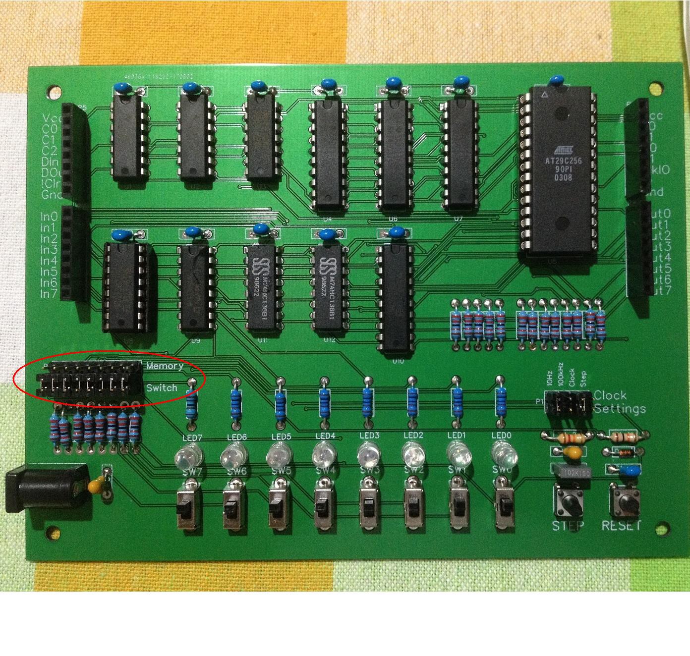
But for this to work all the shunts have to be moved from switch to memory:

With the clock set at 10Hz, it now slow counts away the day.
AlanX
 agp.cooper
Discussions
Become a Hackaday.io Member
Create an account to leave a comment. Already have an account? Log In.