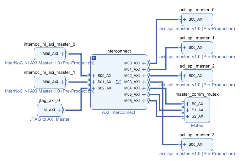
After a few weeks of days of debugging and a few weeks of life getting in the way a first real-case scenario demo of the InterNoC functionality is presented here...
Setup
This log presents a demo of the InterNoC hardware design (see Fig. 1) implemented on a CMOD Artix-7 development board.

In the demo, a master device (STM32 dev. board) is programmed to perform write accesses of different byte count through a UART interface. Two devices were connected to the InterNoC and acted as SPI slave devices:
- An STM32 dev. board
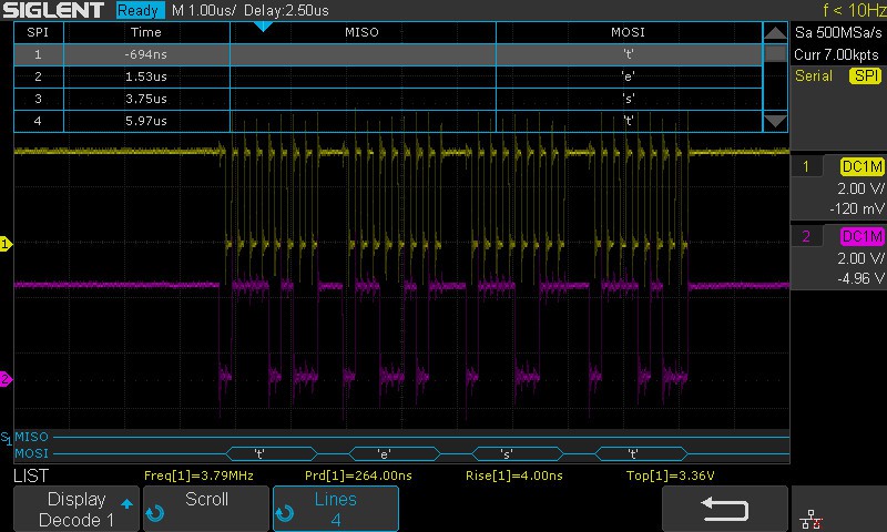
- An oscilloscope with interface decoding capabilities
These devices were chosen in order to facilitate the verification of the InterNoC correct operation. Furthermore, as a means of in-circuit verification the Xilinx Integrated Logic Analyzer (ILA) was used.
The following was defined in-order to communicate using the InterNoC using two mockup messages "ok" and "test" sent respectively to slave 1 and slave 2:
#define INTERNOC_WRITE_CMD 0x0
#define INTERNOC_READ_CMD 0x1

#define INTERNOC_SLV_0 0x0
#define INTERNOC_SLV_1 0x1

// bytecount | access type | slave address in InterNoC
#define INTERNOC_CONSTRUCT_HEAD(byteCount, cmd, addr) ((byteCount << 5) | (cmd << 4) | (addr))

uint8_t write_addr_0 = (uint8_t) INTERNOC_CONSTRUCT_HEAD(0x2, INTERNOC_WRITE_CMD, INTERNOC_SLV_0);
uint8_t write_addr_1 = (uint8_t) INTERNOC_CONSTRUCT_HEAD(0x3, INTERNOC_WRITE_CMD, INTERNOC_SLV_0);

char buffToSend[2] = "ok"; // TX buffer for slave 1
char buffToSend1[5] = "test"; // TX buffer for slave 2
Demo
The master STM32 dev. board was programmed to perform the following loop:
- Write four bytes to slave device in address 0x0
- Wait 2500ms
- Write to two bytes to slave device in address 0x1
- Wait 2500ms
The oscilloscope received correctly the transmitted 4 bytes as presented in the scope capture (see Fig. 2):

Following up is a video of the presented setup running the demo:
 Lefteris Kyriakakis
Discussions
Become a Hackaday.io Member
Create an account to leave a comment. Already have an account? Log In.